
As the chief technologist for the Life Sciences Division at Trane Technologies, Scott Farrar knows a...

Science that is transforming lives and enabling the future
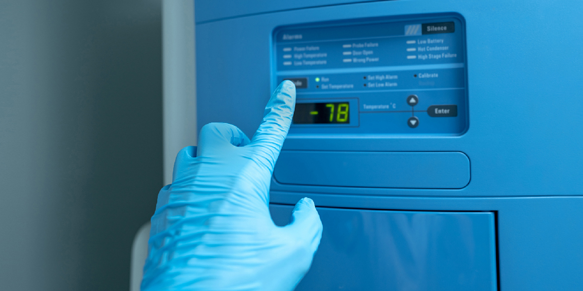
As the chief technologist for the Life Sciences Division at Trane Technologies, Scott Farrar knows a thing or two about ultra-low temperature control for the life sciences industry, perhaps drawing inspiration from his days at Penn State University enjoying peach ice cream. Scott’s biggest inspiration, however, was his entrepreneurial dad who started a solar equipment company, teaching Scott from a young age the importance of sciences, technology, engineering, and mathematics (STEM) education and solving problems. Scott carried those tools with him, and upon completing his formal education, went to work for a pharmaceutical manufacturing company in research and development, specializing in low-temp freezers and incubators as well as heat-momentum and mass-transfer-type processes for the pharmaceutical industry. His exposure to dilemmas and investigative approach is what drove him to create better customer experiences.
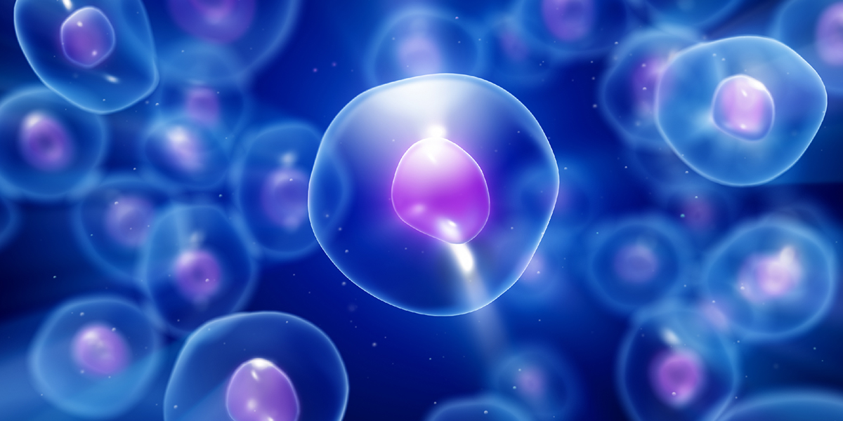
Like the human body, cell and gene therapy is complex. Specialized cells can be lost through age, injury or disease, and such loss cannot always be replenished by healthy cells, rendering the patient extremely sick or even fatally ill. In many cases, the patient has minimal time to live, with very few cells for transplantation. Thanks to advances in both cell and gene therapies, patients have options as these interventions continue to advance. Cellular therapy includes immunotherapies, vaccinations, and cancer vaccines. While gene therapy aims to modify or alter the biological properties of living cells for therapeutic use. As these interventions are distinct, their manufacturing processes often intersect, leaving opportunities for therapeutic enablement.
Inconsistent results and deviation are major issues in cell therapy manufacturing, primarily resulting from historically manual methods, scarcity of proprietary tools, and lack of operator training. With this difficult process also comes another hurdle–time. Providing a safe vein-to-vein transmission is critical when a patient is waiting (in many cases) for lifesaving therapy. How can we bridge the gap between speed, quality, safety, and consistency?
Within the life sciences industry, controlling biological and micro contaminants in process streams is vital to improving operating efficiency and the enablement of technological advances such as modern drug development and monoclonal antibodies (mAbs). Sterile filtration plays a critical role in protecting vital bioprocesses and is the cornerstone in eliminating contaminants. But what happens when a filter gets plugged and how can you minimize impact on filtration performance?
Entegris is proud to collaborate with Kuhner Shaker in the development of a 2500L single-use bag that could exceed their complex requirements while meeting their production needs at scale. Delivering a reproducible product every time, with the ability for specialized applications across scales is what Entegris does best, and this joint effort is no exception. Kuhner evaluated several bag designs for robustness in their 30-day shaking process that were not able to meet the requirements. The Entegris design not only met the need for 30 days of use but was still going strong over 100 days of continuous use.
Entegris is proud to announce a new relationship with Farrar Scientific, by Trane Technologies – a global climate innovator. Farrar offers best-in-class operating systems for ultra-cold temperature storage and controlled rate freeze/thaw chambers for pharmaceutical, biotech, and biorepository applications. Entegris offers the best-in-class Aramus™ bag for robust cold storage and transport. Collaborating with Farrar enables Entegris to offer a combined solution that accelerates the freeze/thaw process.
Entegris is proud to announce a new relationship with HOF Sonderanlagenbau GmbH, an international provider of freeze/thaw equipment and special solutions for the pharmaceutical and biotechnology sectors. Entegris offers the best-in-class Aramus™ bag for robust cold storage and transport.
Whether it is a deliberate strategy or serendipity, the innovations that shape our lives are the result of skilled people put into the right environment to create something new. Innovation is not an exact science, but persistence and some good luck have yielded all the amazing tools and technology we rely upon.
Entegris recently participated at SEMICON West in San Francisco, CA, July 12 – 14. After three years without a major onsite presence, the team was eager to be back in person and engage face-to-face with key customers and suppliers.
Like Benjamin Franklin once stated, “An ounce of prevention is worth a pound of cure.” This could be said for mitigating risk to storage of your biologics too. Even the slightest temperature change from a freezer door being opened and closed numerous times to setting alarms off while searching for product hidden inside can compromise drug product. Losing time and money over product can be prevented. Here are some tips to keep your biologics viable in both long- and short-term freezer storage.
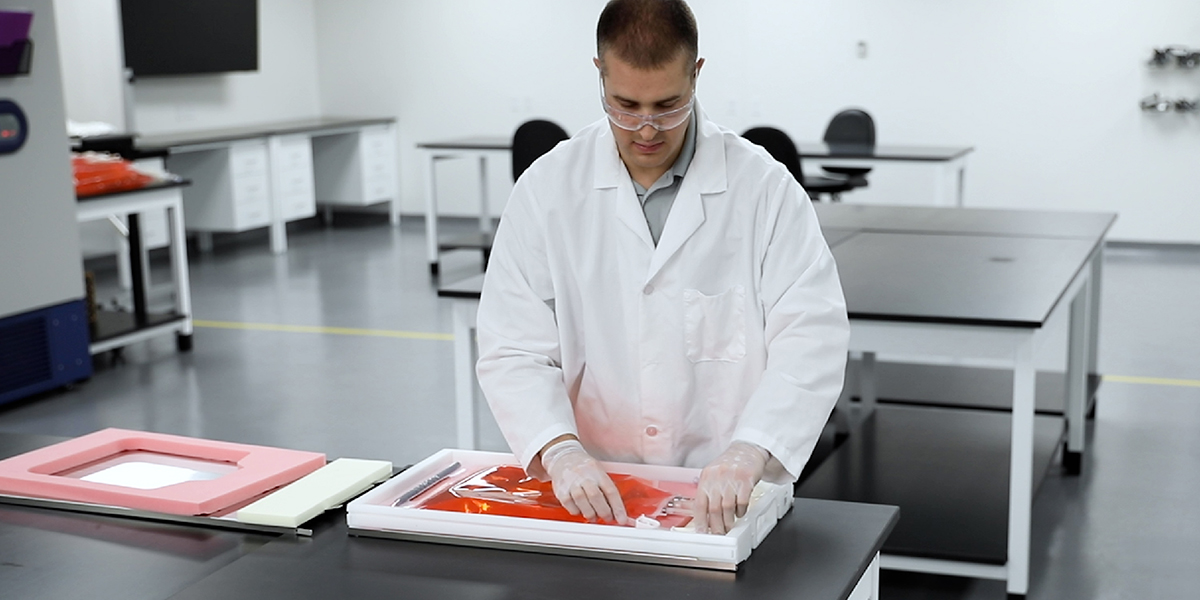
Protecting your product throughout the freeze/thaw process can be a delicate task. Freeze too slowly, your proteins may aggregate and degrade. Thaw in a water bath, you might encounter contamination. Most commonly, cryo-concentration, where your protein is not evenly distributed throughout your frozen container, poses a risk to critical product quality attributes. There are countless ways improper freeze/thaw processes can ruin sensitive therapeutics and cell and gene therapies, but the proper tools can help you reduce cryo-concentration and bioburden while achieving the best return on investment and optimization of your process.
The great resignation, retirement, and an increase in remote work have caused instability across every industry, this is especially true in cell and gene therapy. Getting critical therapies to market has been increasingly difficult due to the high demand for team members with experience in this area, so what can companies do to help combat this?
As the chief technologist for the Life Sciences Division at Trane Technologies, Scott Farrar knows a...

Like the human body, cell and gene therapy is complex. Specialized cells can be lost through age, in...

Inconsistent results and deviation are major issues in cell therapy manufacturing, primarily resulti...

Within the life sciences industry, controlling biological and micro contaminants in process streams ...
Entegris is proud to collaborate with Kuhner Shaker in the development of a 2500L single-use bag tha...
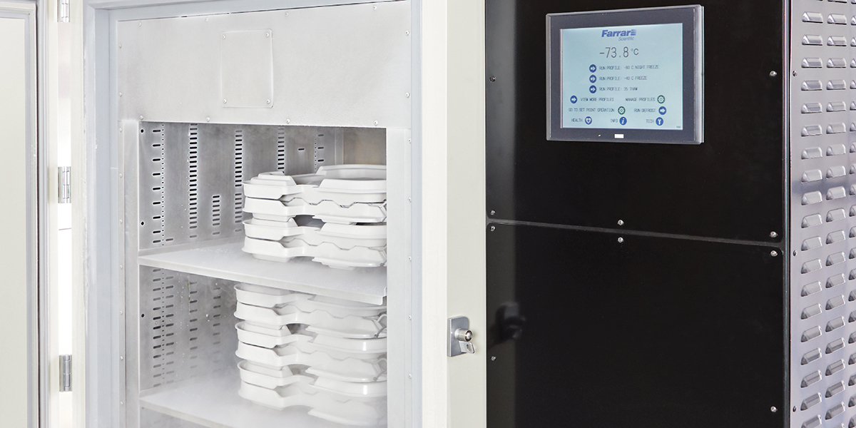
Entegris is proud to announce a new relationship with Farrar Scientific, by Trane Technologies – a g...
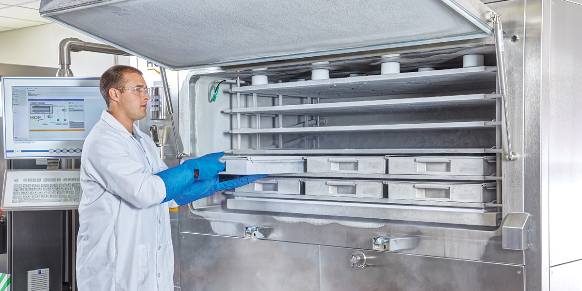
Entegris is proud to announce a new relationship with HOF Sonderanlagenbau GmbH, an international pr...

Whether it is a deliberate strategy or serendipity, the innovations that shape our lives are the res...

Entegris recently participated at SEMICON West in San Francisco, CA, July 12 – 14. After three years...
Like Benjamin Franklin once stated, “An ounce of prevention is worth a pound of cure.” This could be...
Protecting your product throughout the freeze/thaw process can be a delicate task. Freeze too slowly...

The great resignation, retirement, and an increase in remote work have caused instability across eve...
© 2026 Entegris. All Rights Reserved

