
Building Resilient Infrastructure to Better Serve Our Customers: A Vision from Abhijeet Bhandare “Ou...

Science that is transforming lives and enabling the future
Building Resilient Infrastructure to Better Serve Our Customers: A Vision from Abhijeet Bhandare “Our digital transformation is about one thing: being the most reliable, innovative partner for our customers.” – Abhijeet Bhandare
Silicon Carbide’s Next Phase: From Expansion to Optimization
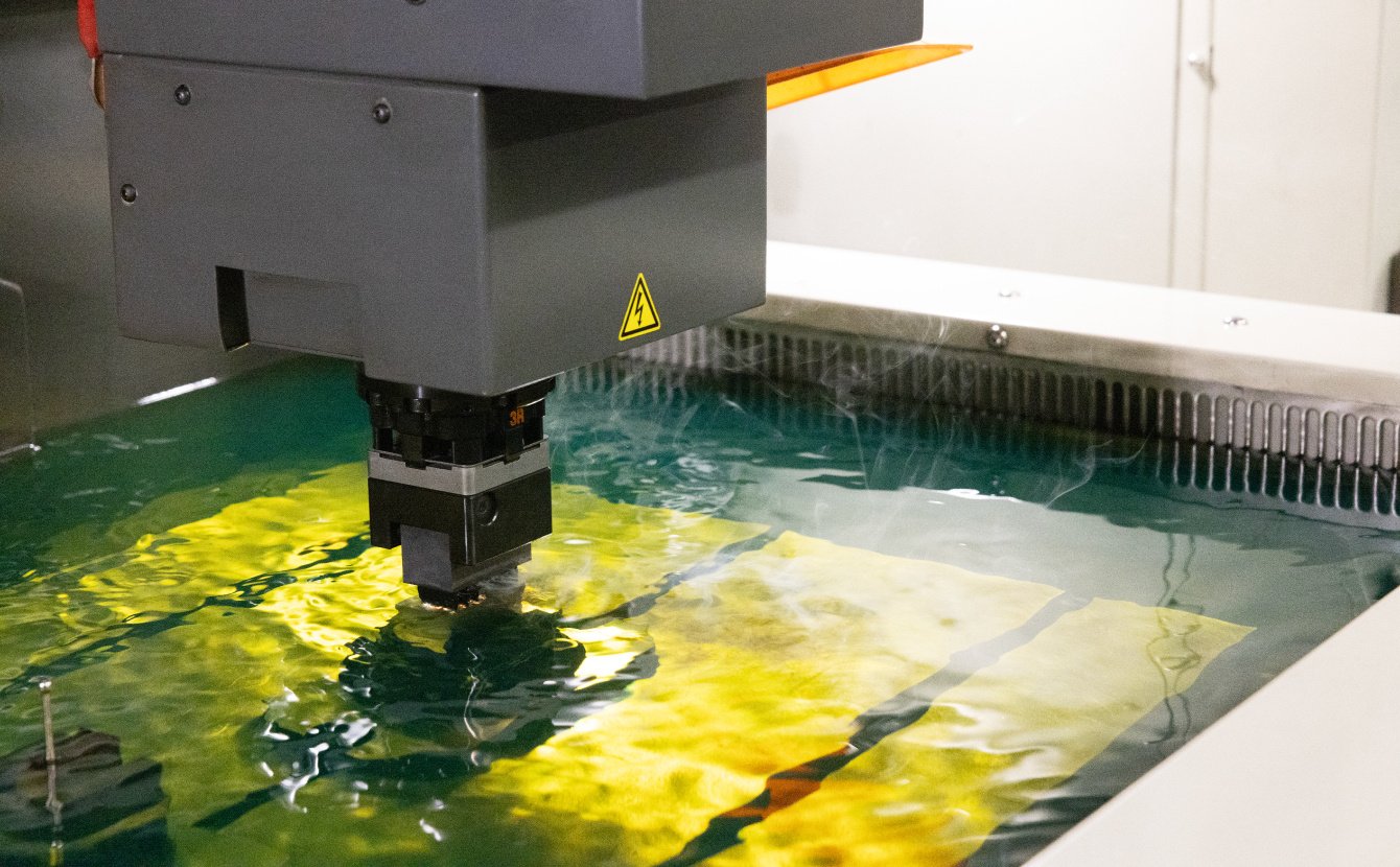
Sustainability Challenges Around SiC Polishing Slurry recycling supports cleaner semiconductor manufacturing
What does an Entegris employee look like? What do they do all day, and what do they like about their jobs? This is part of a series that will take a deep dive into a variety of careers at Entegris. We’ll highlight several employees and their valuable contribution to the organization. What do they do, how are they succeeding, and why do they think Entegris is a great place to work?
The Future of Silicon Carbide Manufacturing: Innovations and Techniques
Minimizing Particulates in Single-Use Systems Operators need to take extreme care when closing their single-use systems. That’s because particulates in single-use components are under increasing regulatory scrutiny. Particulates can also impact the biomanufacturing, storage, and transportation of high-value final products. These concerns can bring a halt to drug manufacturing and delay patients from getting the medicines they need.
Exploring Entegris POCO Materials EDM-1® Graphite
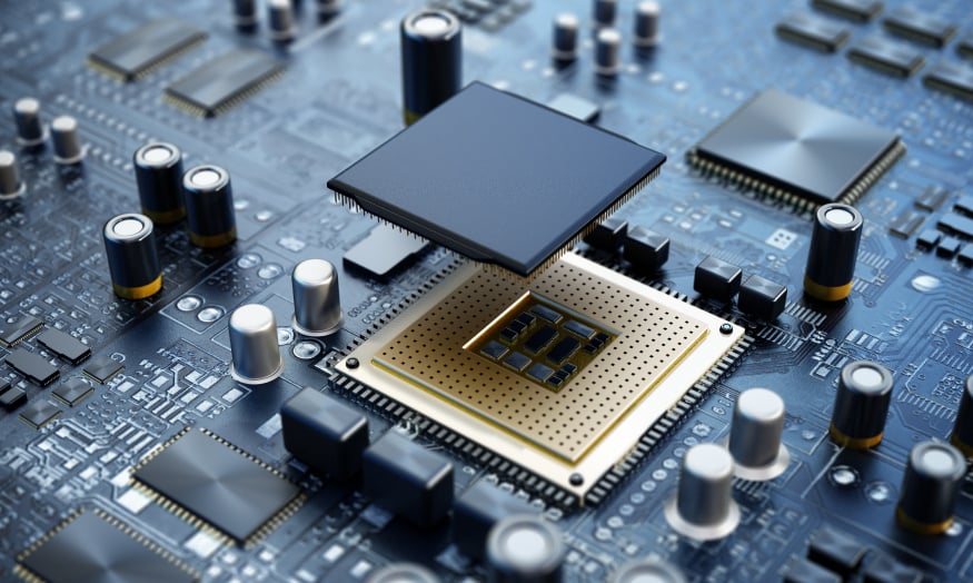
Empowering Semiconductor and Device Performance with Improved Point-of-Use Filtration
What does an Entegris employee look like? What do they do all day, and what do they like about their jobs? This blog is part of a series that will take a deep dive into a variety of careers at Entegris. We’ll highlight several employees and their valuable contributions to the organization. What do they do, how are they succeeding, and why do they think Entegris is a great place to work?
Driving the Future with SiC The semiconductor industry is abuzz with discussions around silicon carbide (SiC) — a material poised to revolutionize power electronics. Global megatrends like sustainability, the rise of electric vehicles, and the growing demands of AI systems have made SiC essential for enabling efficient, high-performance solutions. At Entegris, we’ve embraced this momentum, working with industry-leading chipmakers to help make an impact in the SiC space. Here’s a review of some of our exciting work around SiC over the past year.
Advancing Space Domain Awareness: MIT Lincoln Laboratory's Innovative Mirror Technology and the Role of Entegris SUPERSiC®-SP Enhancing our understanding of the space environment is crucial to navigating the ever-evolving landscape of space exploration. As part of collaboration efforts between the U.S. and Japan to boost space domain awareness through cutting-edge mirror technology, MIT Lincoln Laboratory (MIT LL) built payloads hosted on Japanese satellites. MIT LL built two identical space payloads for the Japanese QZS-6 and QZS-7 satellites and selected Entegris’ SUPERSiC-SP silicon carbide (SiC) material to serve as a substrate for their mirrors. They also chose our chemical vapor deposition (CVD) SiC solution to serve as a mirror cladding. These payloads are part of a collaborative effort between the U.S. and Japan to augment space domain awareness of objects in or near geosynchronous orbit (GEO). This initiative not only showcases international cooperation but also highlights the innovative engineering challenges and solutions involved in creating functional space payloads.
Building Resilient Infrastructure to Better Serve Our Customers: A Vision from Abhijeet Bhandare “Ou...

Silicon Carbide’s Next Phase: From Expansion to Optimization

Sustainability Challenges Around SiC Polishing Slurry recycling supports cleaner semiconductor manuf...

What does an Entegris employee look like? What do they do all day, and what do they like about their...
Looking Back at 60 Years of Moore’s Law
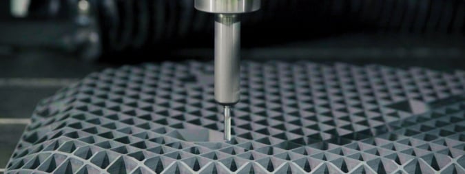
The Future of Silicon Carbide Manufacturing: Innovations and Techniques

Minimizing Particulates in Single-Use Systems Operators need to take extreme care when closing their...
Exploring Entegris POCO Materials EDM-1® Graphite

Empowering Semiconductor and Device Performance with Improved Point-of-Use Filtration

What does an Entegris employee look like? What do they do all day, and what do they like about their...

Driving the Future with SiC The semiconductor industry is abuzz with discussions around silicon carb...
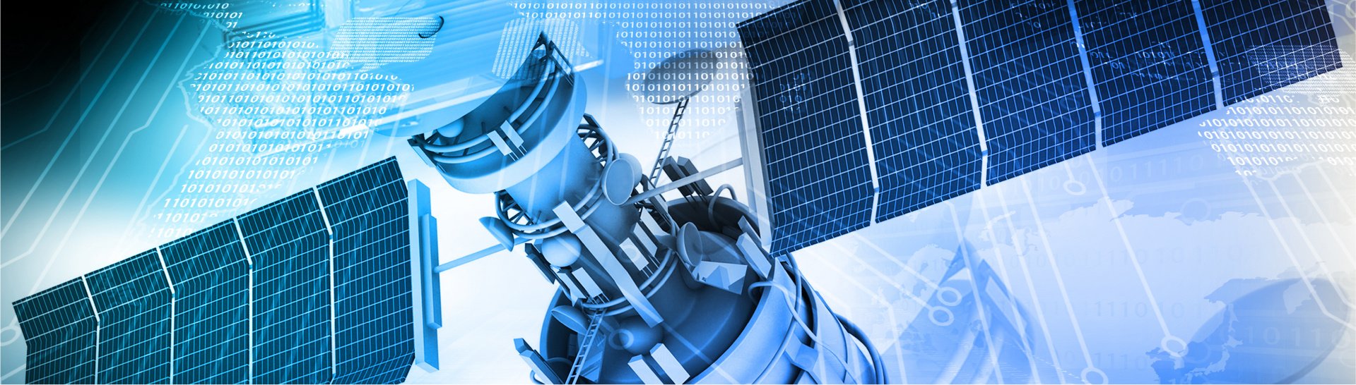
Advancing Space Domain Awareness: MIT Lincoln Laboratory's Innovative Mirror Technology and the Role...
© 2026 Entegris. All Rights Reserved

