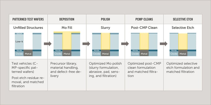
Changing one material in the semiconductor manufacturing process has a cascading effect on multiple process steps. Consider the replacement of tungsten (W) and copper (Cu) with molybdenum (Mo). Integrated device manufacturers (IDMs) are implementing Mo in advanced designs, focusing on 2-nanometer (nm) nodes and below. Mo is highly conductive, can be deposited without a titanium or titanium nitride barrier layer, and is cost-effective compared to other alternatives. But its susceptibility to corrosion introduces new challenges for deposition, etch, and many other process steps.
How does switching to Mo influence other semiconductor process steps?

Tailoring the CMP Process
Chemical mechanical planarization (CMP) is a critical process step that is required for multiple layers of metals and oxides. Slurries, pads, pad conditioners, cleans, and other materials optimized for W or Cu need to be modified to protect Mo against corrosion during CMP.
Slurries for metal CMP are typically formulated with an oxidizer such as hydrogen peroxide (H2O2). The H2O2 concentration in advanced Mo slurries is significantly less than 1%, making precise control especially important.
Pad design is also important for a corrosion-prone metal like Mo. The top layer of the pad can be customized to significantly improve scratch performance without sacrificing planarization and Mo removal rate. Customized groove patterns that aid in the slurry transport beneath the wafer also improve performance while minimizing the risk of damage.
Word Line Etching
Word line etching for 3D NAND structures is a prime example of an application where using processes developed for W do not transfer to Mo. In a Mo-filled structure, the recess interacts differently with etchants and cleans. Top-to-bottom uniformity often suffers when using typical etchants like phosphoric acid/acetic acid/nitric acid (PAN). Conventional acidic or alkaline cleans can leave Mo residue on the side walls and result in local inconsistent Mo etching from layer to layer.
Selective high-performance etchants customized for Mo offer a better-performing alternative. These formulations combine etching and cleaning in a single step. They are available in acidic or alkaline versions that do not leave residues and enable longer bath life and shelf life.
High-Purity Materials and Filtration for Higher Yield
Maximizing yield starts with the incoming materials. For Mo deposition, chlorine-based halide precursors are preferred to avoid the carbon contamination that can occur with common liquid precursors. These molybdenum chloride materials are solids at room temperature and must be sublimated for delivery to the wafer. High-purity powder sources are the first step in ensuring contamination-free deposition.
- High purity incoming raw materials are only one aspect to consider for high yield. Contamination can occur at any point. In situ monitoring and process adjustments when indicated will improve consistency and yield.
- Adequate filtration is necessary for high yield in any process. Filtration needs to happen at multiple process steps for advanced nodes where contaminants as small as 20 to 30 nm can cause yield loss.
- CMP slurry filtration is helpful both in the recirculation loop and at the point of use. Multiple filtration steps remove any large particles of the slurry abrasive that have agglomerated. These also filter out contaminants, including fine particles.
Filters are also critical for pCMP processes. A supplier that provides both cleaning chemistries and filters can recommend the best combination to optimize filtration performance and filter lifetime.
Looking at the Big Picture
When transitioning to Mo, IDMs need to accelerate speed-to-yield to run a high-purity process as quickly as possible. It can be difficult to select an appropriate combination of chemicals, pads, filters, and handling equipment to minimize oxidation risk and maximize yield. Close collaboration between IDMs and suppliers is necessary but may not be sufficient.
If IDMs purchase various materials from multiple suppliers, they must conduct additional testing to fully understand interactions between all the materials used throughout the fab. When a single supplier offers deposition, precursors, CMP chemicals and materials, etchants, wafer handling, and filtration media, they have tested these materials for compatibility. There are also fewer parties involved, so transition and material selection may proceed faster. Choosing an experienced supplier that offers high-quality materials for multiple process steps smooths the changeover and accelerates the path to high yield.
For more information about the transition to Mo, see our white paper, “Migrating to Molybdenum: Comprehensive IC Solutions to Streamline the Transition.”


