

DRAM architecture has remained virtually unchanged for the past decade, with the dimensions shrinking proportionally with each successive device node. This linear path, however, is reaching its limits for nodes below 20 nanometers (nm) including 1x, 1y, 1z, 1a, and 1b. A major change will be needed soon if DRAM is to keep up with advances in logic.
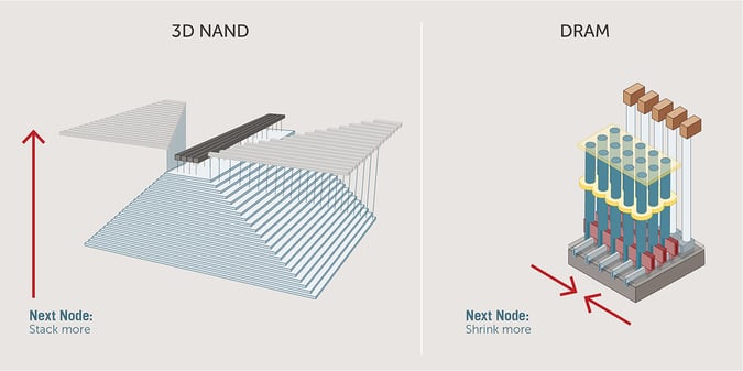
DRAM lies near the top of the memory hierarchy pyramid1 where its proximity to the central processing unit (CPU) makes performance paramount. Unlike NAND, where cost-per-unit-cell drives innovation, fast switching speed must be prioritized. Scaling DRAM devices has, thus far, been accomplished much like scaling logic, where advances require shrinking the device dimensions rather than stacking vertical structures as has occurred with non-volatile 3D NAND memory, Figure 1.
DRAM, which consists of a transistor and a capacitor, Figure 2, is a volatile memory, meaning that data is lost when power is shut off to the cell. For DRAM, the charge in the capacitor leaks away over time so the cells need to be charged every few milliseconds from a separate power source. In contrast, non-volatile memory relies on charge-trapping materials like silicon nitride or a confined conductor such as polysilicon to hold the charge within the cell.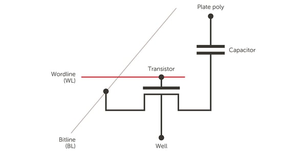
FOCAL POINTS FOR FUTURE DRAM DEVELOPMENT
Next-generation DRAM cells will need new materials and architectures to address the challenges that device shrinking poses. As layer thickness or line width decreases below a threshold value, the electrical resistivity of metal lines increases dramatically and nonlinearly due to surface scattering, film roughness, and grain boundary defects.1 Tungsten (W) has thus far remained the standard choice, but new materials are now being evaluated to minimize the increase of effective resistance with shrinking dimensions. The capacitor will likely change from a cylinder type to pillar type, necessitating material property improvements.
As cell size shrinks, crosstalk between adjacent cells becomes a greater concern. One method to address this issue involves placing an air gap between bitlines to minimize parasitic capacitance. Inter-metal dielectrics (IMD) with a low dielectric constant also minimize crosstalk. Common low-κ dielectrics are more porous than their predecessors, requiring molecular precursors not usually associated with DRAM manufacturing.
PHOTOLITHOGRAPHY CHALLENGES AND PATTERNING
Shrinking DRAM dimensions are imposing changes in lithography patterning and exposure. For example, controlling critical dimensions during deposition and etching steps of self-aligned double patterning (SADP) causes a pitch-walking effect. Introducing extreme ultraviolet lithography (EUVL) or applying self-aligned quadruple patterning (SAQP) are two approaches being considered to alleviate the pitch-walking effect that becomes more severe at the 1x node, as spacing approaches the imaging resolution limit of 193i lithography.
The maximum allowed size of killer and latent defects reduces with each advancing node. Aggressive measures are needed to reduce the prevalence of these defects for 1x, 1y, and 1z devices. It is prudent for all advanced devices to have in place a filtration and purification strategy to avoid liquid and gas phase contamination entering the process materials.2
Metallic contamination related to chemical mechanical polishing (CMP) is especially critical for DRAM since CMP steps are occurring very close to the transistor. CMP of W at smaller dimensions needs sophisticated slurries that require post-CMP cleaning. Cleaning chemistries must be tailored to the CMP process for adequate residue removal.
POTENTIAL FOR DISRUPTIVE CHANGES
DRAM manufacturers are working to develop structures that will accommodate the needs of the 1y, 1z, and 1a nodes and beyond. Such developments may involve changes in materials and processes but may also require innovative and disruptive solutions. Envisioned disruptive solutions either alter the DRAM architecture, (e.g., 3D transistor) or incorporate different memory technology into DRAM devices.
Several emerging memory technologies,3 including phase change memory (PCM) and multiple RAM variants are in various states of maturity and all have the advantage over DRAM of being non-volatile. But despite improvements in speed and endurance some have not succeeded in replacing DRAM due to high cost.4 However, given the industry trend to bring logic and memory closer together to improve latency and create memory cells that perform logic tasks, emerging memory technologies may take hold.
SUMMARY
DRAM fabrication will need to evolve to meet the demands of high-performance devices over the next few years. Next-generation DRAM cells will need new materials and architectures to address the challenges that device shrinking poses.
Solutions range from replacing the wordline metal to completely rethinking device architecture. Making significant changes will require chipmakers to carefully consider tradeoffs between, speed, cost, and endurance.
To learn more, download the full white paper, DRAM Device Fabrication: Material Challenges.
References
1 Considerations for Improving 3D NAND Performance, Reliability, and Yield, Entegris white paper, September 2018. https://info. entegris.com/white-paper-considerations-for-improving- 3d-nand-performance-yield-and-reliability
2 Colligan, N., Uncovering Chemical Quality Improvements through a Holistic Approach to Chemical Quality Management Contamination Free Manufacturing, 2018 29th Annual SEMI Advanced Semiconductor Manufacturing Conference (ASMC), Saratoga Springs, NY, 2018, pp. 286-290.
3 Chen, A., Solid State Electronics 125 (2016) 25-38.
4 Storage Class Memory: Advances in Materials and New Device Architecture Improve Cost of Ownership for High-Density Phase Change Memory, Entegris white paper, January 2020. https://info. entegris.com/storage-class-memory-advances-in-materials-new-device-architecture-for-high-density-phase-memory-wp.

