Changing one material in the semiconductor manufacturing process has a cascading effect on multiple ...

Science that is transforming lives and enabling the future
Changing one material in the semiconductor manufacturing process has a cascading effect on multiple process steps. Consider the replacement of tungsten (W) and copper (Cu) with molybdenum (Mo). Integrated device manufacturers (IDMs) are implementing Mo in advanced designs, focusing on 2-nanometer (nm) nodes and below. Mo is highly conductive, can be deposited without a titanium or titanium nitrid
Silicon carbide (SiC) has become popular with chipmakers. Its wide-bandgap structure offers many design benefits for the operations of power semiconductors. Compared to silicon, SiC wafers enable the fabrication of faster, more efficient devices that can both operate at higher temperatures and remain stable when deployed in extreme temperature environments. Processing SiC wafers using the same materials and methods as silicon wafers is not a viable option, however.
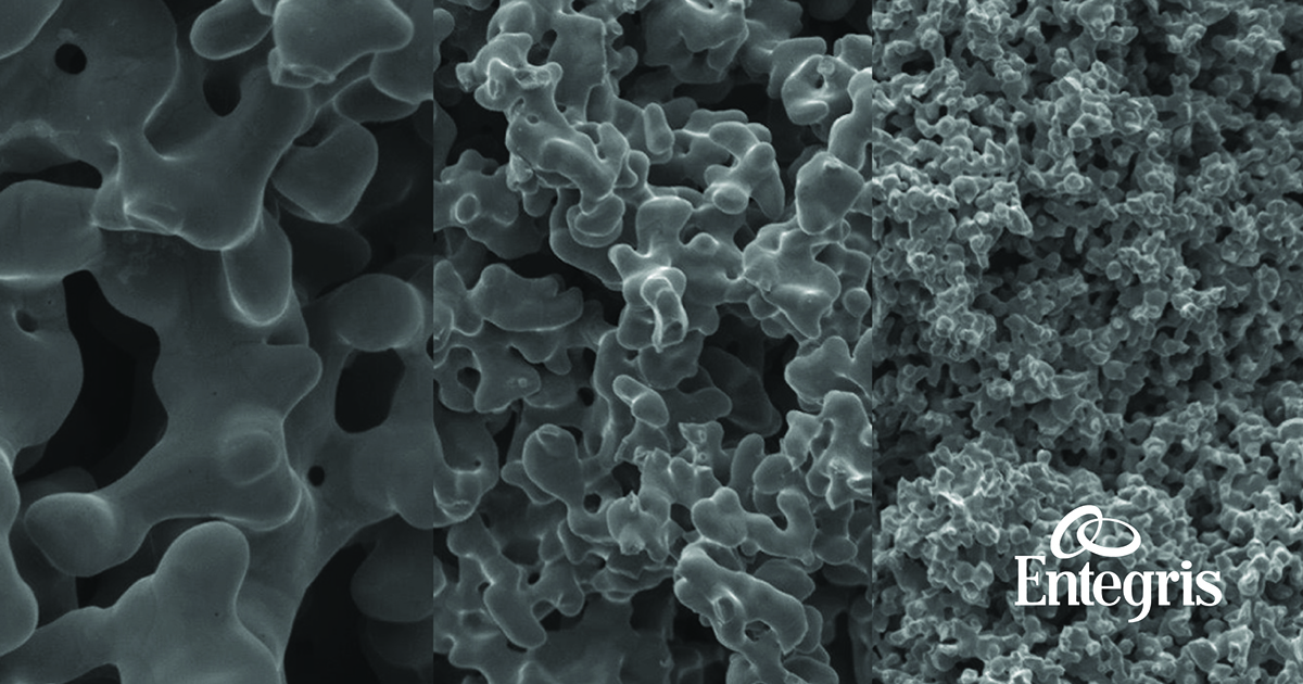
If you asked a semiconductor process engineer to name their biggest challenge when tackling the next technology node, they would likely tell you it is figuring out how to achieve high device yields. This is mainly due to an increase in possible points of contamination as the number of potential contaminants grows and their sizes shrink. It is becoming particularly difficult to detect metal contaminants and pinpoint their root cause so they can be eliminated. That’s because they can form anywhere in the process flow.
In the early days of semiconductor manufacturing, fabs would remove contaminants from their process fluids in a sequence that could be analogized to making a cup of coffee. By using a filter with tiny pores, large contaminants (coffee grounds) are separated from water. Because the coffee grounds are too large to pass through the filter, they can’t pass into the coffee we drink.
For decades, the semiconductor device manufacturing mantra was “How do we make them smaller, cheaper, and faster?” The pursuit of Moore’s Law – the doubling of transistors on a chip every two years – was achieved through planar scaling. But that approach could only go on for so long. The mantra now is “How do we improve power, performance, area, and cost (PPAC)?” At the 14 nm node, it was clear that the best way to push the limits of semiconductor device PPAC was to take it into the third dimension.
Things are not always as they appear. Take semiconductor manufacturing. On the surface, it may seem that the secret to making semiconductor devices more advanced lies in the design. But just as an architect’s design for a building may not be structurally feasible without the right materials, a semiconductor device design may not be functional if the materials and their interactions are not considered and optimized.
Here’s a challenge, say the number 9 out loud, nine times. 9, 9, 9, 9, 9, 9, 9, 9, 9.
Whether it is a deliberate strategy or serendipity, the innovations that shape our lives are the result of skilled people put into the right environment to create something new. Innovation is not an exact science, but persistence and some good luck have yielded all the amazing tools and technology we rely upon.
Entegris recently participated at SEMICON West in San Francisco, CA, July 12 – 14. After three years without a major onsite presence, the team was eager to be back in person and engage face-to-face with key customers and suppliers.
A major difference exists as more features from our smartphones are integrated, replicated, and expanded in our cars - reliability expectations. A smartphone is designed to work effectively for 3-5 years while cars expect 10-15 years with standard maintenance. Failure in our cars can create dangerous situations for drivers, passengers, and others on the roadway. Designing and manufacturing our cars to ensure the functional safety along with the performance expectations of our new digital transportation systems is challenging manufacturing models for carmakers.
The expanding need for massive data storage and processing has driven the migration from 2D to 3D architectures for logic and memory chips. These complex architectures, with their high aspect ratio (HAR) designs and ultra-thin layers, are forcing advances in metal and oxide deposition processes. Atomic layer deposition (ALD) is usually the method of choice for producing uniform layers with precisely controlled composition.
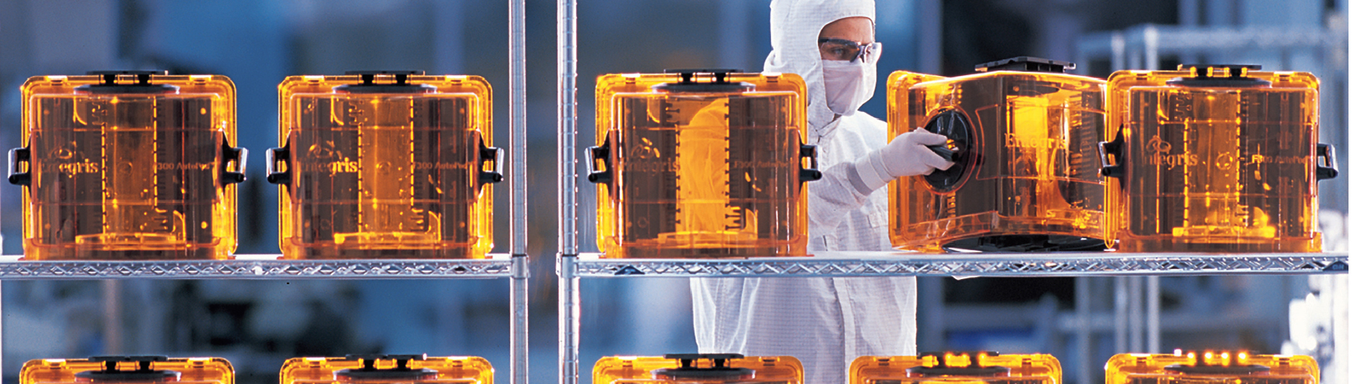
Beyond being one of the fun words in the semiconductor industry, the “FOUP,” front-opening-unified-pod, represented a radical change that has influenced the productivity of each fab and contributed to the capabilities our electronic devices today. At the inception of Moore’s Law in 1965, 30 mm (1.25”) diameter wafers were the standard. Leading up to the late 1990’s, seven generations of incremental increases would be introduced. At each point, manufacturing efficiencies and device performance opportunities existed to get “Moore” out of each wafer. Wafer storage and transport was primarily accomplished in open-air cassettes and pods, leaving wafers more susceptible to physical damage and contamination.
Changing one material in the semiconductor manufacturing process has a cascading effect on multiple ...

Silicon carbide (SiC) has become popular with chipmakers. Its wide-bandgap structure offers many des...

If you asked a semiconductor process engineer to name their biggest challenge when tackling the next...

In the early days of semiconductor manufacturing, fabs would remove contaminants from their process ...

For decades, the semiconductor device manufacturing mantra was “How do we make them smaller, cheaper...

Things are not always as they appear. Take semiconductor manufacturing. On the surface, it may seem ...
Here’s a challenge, say the number 9 out loud, nine times. 9, 9, 9, 9, 9, 9, 9, 9, 9.

Whether it is a deliberate strategy or serendipity, the innovations that shape our lives are the res...

Entegris recently participated at SEMICON West in San Francisco, CA, July 12 – 14. After three years...

A major difference exists as more features from our smartphones are integrated, replicated, and expa...

The expanding need for massive data storage and processing has driven the migration from 2D to 3D ar...
Beyond being one of the fun words in the semiconductor industry, the “FOUP,” front-opening-unified-p...
© 2026 Entegris. All Rights Reserved

