

 Since the introduction of the mobile phone, scientists and engineers have been on a series of quests to make them smaller and smarter. And incarnation after incarnation, from shoe box large to smart phone tiny, they succeeded. Until, that is, demand for more data, more storage, faster speeds, and longer battery life created major roadblocks. New smartphone capabilities — from biometrics to more accurate geopositioning, from artificial intelligence to virtual reality — demanded significant improvements in chip power. Their constant use required pronounced leaps in battery life.
It’s been a fascinating odyssey for Entegris working hand-in-hand with semiconductor manufacturers to find their way around these roadblocks. It required engineers to overcome not only multiple scientific hurdles but also significant problems of marketing and logistics. What is especially fascinating in the scientific community is how advances in one area – in this case logic technology – leads to similar gains in others – memory.
Ironically, until relatively recently, making improvements was comparatively simple – at least by present-day standards. Advances in photolithography allowed not only more transistors but also more highly sophisticated transistors — the phones’ brains — to be fabricated onto silicon wafers.
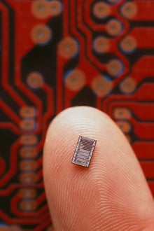 It reached a point where semiconductor fabricators were able to place 15 billion transistors – 15 billion – on a piece of silicon no larger than a thumbnail. To achieve this level of density, however, required working with 5 nanometer node processing technology. A nanometer is one-billionth of a meter. At that size, the technology had reached a point, where – at least according to conventional wisdom – the only way to add more transistors was to increase the size of the chip – an unacceptable solution. You don’t make phones smaller by increasing the size of their internal workings.
But as Wenge Yang, Ph.D., and Entegris vice president of market strategy points out, “In our industry, we set a goal, we make significant investments in R&D, and create large, focused teams of engineers to solve the problem. They never fail to make it happen. They find the solution no matter how complex the challenge.”
The idea the scientists came up with for the smartphone dilemma was simple: If you can’t build out in size, perhaps you can build up. In retrospect, the idea may seem obvious. But certainly, the execution was not.
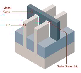 Essentially the new 3D architecture, built on a FinFET device, has numerous advantages. Moving out of the flat plane of a silicon wafer into a vertical dimension allows for better performance at lower power levels. But – and there is always a but – the new device architecture required new materials with increasingly stringent – and difficult to meet – performance standards for proper fabrication.
In other words, while FinFET opened a new world of semiconductor fabrication, it also opened a new world of potential problems. For example, with transistors outside the plane of the wafer, films such as the hafnium oxide (HfO2) gate dielectric must have extremely low levels of impurities. Entegris developed a new manufacturing procedure for the film that is so unique a patent is pending on the process solving at least that problem.
But there were others. If film thickness was not applied absolutely evenly, device leakage became another problem. Even the slightest variation in the hafnium oxide (HfO2) gate dielectric can adversely impact it. Also, thickness variations across the chip broaden the threshold voltage distribution, making it difficult to turn off the 16-billion-plus transistors all at once. This in turn led to the increased use of the atomic layer deposition (ALD) processes, a technique where materials are deposited on the wafer just a few atomic layers at a time and in a sequential manner.
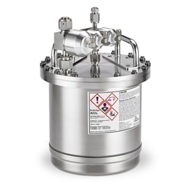 It is actually even more complicated than it sounds. Because of HfO2 gate dielectric’s extreme sensitivity to impurities, the traditional metalorganic precursors – usually gases or liquids – used in ALD didn’t work. What did work and became the preferred precursor is a solid at room temperature, complicating delivery further. It is more corrosive, has low vapor pressure and has a tendency to deposit particulates. So, it was back to the drawing board, which is where Entegris developed its patented ProE-Vap® delivery system designed for solid-state precursors used in ALD and chemical vapor deposition (CVD).
In summary, these solutions may appear to have materialized very easily. But they are actually the result of thousands of man hours of work, of trial and error, back to the drawing boards and occasional frustration. It was a process in some ways reminiscent of Thomas Edison’s experiments in search of the best filament for the light bulb.
The filament, in this case, was a very specific combination of molecules. Batch by batch, samples were sent to the customer for testing. There, the fabricator went through a series of carefully orchestrated steps that began by checking whether the molecules could successfully be placed on a wafer. After the wafer was processed, it had to be checked to assure the transistors work. By work, the standard was do they work faster than current transistors and use less energy.
If not, start again. How close were we? What needs to be changed? On and on over five years and hundreds of tests, until the molecule is perfect.
But even a so-called “perfect” molecule may not be perfect. Yes, it passes the fab test – it’s fast and energy efficient – when placed on a single wafer in an experimental lab. But will it stand up to mass production when hundreds of wafers must be processed every hour?
Another consideration is final price. Will a higher outlay for materials boost the cost of phones to an unacceptable level? Very simply: costs have to be in line with the previous generation. Consumers won’t stand for, say, a ten-fold price increase.
Also, are the materials widely available? Will the well- publicized supply chain problems impact both production and cost? Will manufacturers need to build new facilities or extensively modify those that already exist?
 To add another layer or concern: will the process require re-tooling? How many million-dollar machines need be designed, developed, and purchased? And how will that impact costs?
The need for precision is paramount because the consequences of any error are significant. If something goes wrong, you have to shut down the line, throw out all the wafers potentially impacted at literally a cost of billions.
Similar problems were encountered increasing DRAM when chip density became greater than lithographic capabilities. Again, after much trial and error, Entegris developed filters and technology that allows for the smooth operation of 3D flash NAND chips that currently have more than 100 layers.
The irony, of course, is that once everything is perfected, it’s just a matter of time before the industry moves on in search of the next problem to solve.
Read more about the semiconductor innovations that power smartphone technology in Entegris’ 2021 Scientific Report.

