
Entegris is delighted to announce our new interactive tool intended to help the life sciences indust...

Science that is transforming lives and enabling the future
Entegris is delighted to announce our new interactive tool intended to help the life sciences industry better understand how we can support the entire drug manufacturing process. Our growing life sciences portfolio can be overwhelming for customers, and this simple tool helps guide them to finding all the ways we can help. The tool was designed to be versatile and can be shared by our team as part of a sales overview, or you can explore it yourself to quickly learn more about the solutions we offer.
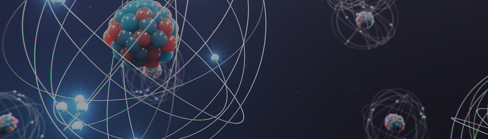
If you asked a semiconductor process engineer to name their biggest challenge when tackling the next technology node, they would likely tell you it is figuring out how to achieve high device yields. This is mainly due to an increase in possible points of contamination as the number of potential contaminants grows and their sizes shrink. It is becoming particularly difficult to detect metal contaminants and pinpoint their root cause so they can be eliminated. That’s because they can form anywhere in the process flow.
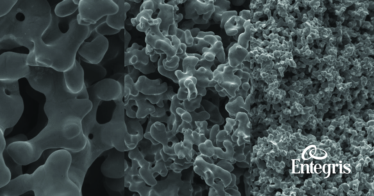
In the early days of semiconductor manufacturing, fabs would remove contaminants from their process fluids in a sequence that could be analogized to making a cup of coffee. By using a filter with tiny pores, large contaminants (coffee grounds) are separated from water. Because the coffee grounds are too large to pass through the filter, they can’t pass into the coffee we drink.
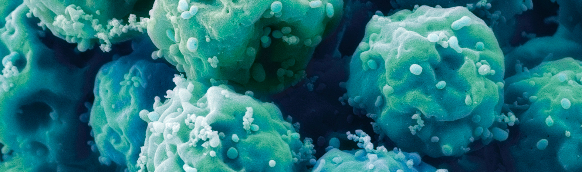
Biopharma manufacturing is an essential part of the healthcare industry, producing lifesaving treatments for patients around the world. Traditional manufacturing methods can have a significant environmental impact driven by stainless steel equipment requiring extensive cleaning and sterilization processes that consume substantial amounts of water and energy in addition to cleaning agents.
For decades, the semiconductor device manufacturing mantra was “How do we make them smaller, cheaper, and faster?” The pursuit of Moore’s Law – the doubling of transistors on a chip every two years – was achieved through planar scaling. But that approach could only go on for so long. The mantra now is “How do we improve power, performance, area, and cost (PPAC)?” At the 14 nm node, it was clear that the best way to push the limits of semiconductor device PPAC was to take it into the third dimension.
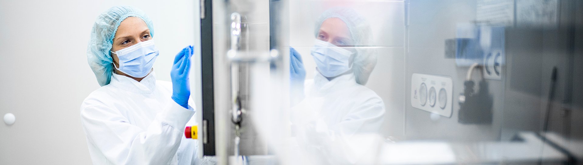
Entegris is delighted to announce our collaboration with Agilitech, a pioneering partner to the biotech industry. Agilitech provides highly flexible, scalable, and future-proof single-use technologies for every step of the bioprocess. These include chromatography systems, mixers, and custom-tailored bioprocess controllers that scale from the laboratory to commercial production environments. This makes them a natural fit for the unique needs of life sciences customers.
Things are not always as they appear. Take semiconductor manufacturing. On the surface, it may seem that the secret to making semiconductor devices more advanced lies in the design. But just as an architect’s design for a building may not be structurally feasible without the right materials, a semiconductor device design may not be functional if the materials and their interactions are not considered and optimized.
By: Mike Lamach, Reach-In Sales Leader, FARRAR™ | Trane Technologies The explosion of needs for -80°C through -60°C assets over the past decade has been nothing short of remarkable. Clinical research investments keep expanding while commercial-scale needs continue to transform the landscape.
HOF Sonderanlagenbau GmbH has been a leader in freezer technology since 1988 under founders Hans-George Hof and Herrmann Schäfer in Lohra, Germany. Through technical knowledge and entrepreneurship, HOF has grown into a global freezer and service operation, specializing in freeze-drying systems for the pharmaceutical and biotechnology industries, serving 28 countries, with 40 customer sites and more than 100 freeze/thaw units serving the biotech and pharmaceutical market.
Whether you’re new to cold chain or a seasoned freeze/thaw pro, it can be difficult to find value-driven solutions for configuring freeze/thaw (F/T) biologic treatments and therapies. Complex cold chain demands are not one-size-fits-all and your team’s time is precious, which is why we created our Cold Chain Guidance Tool. This innovative tool guides you through common decision-making scenarios, analyzes your inputs, and provides you with an assessment of the biggest drivers to achieve optimal results from your process.
Here’s a challenge, say the number 9 out loud, nine times. 9, 9, 9, 9, 9, 9, 9, 9, 9.
Entegris is delighted to announce our new interactive tool intended to help the life sciences indust...

If you asked a semiconductor process engineer to name their biggest challenge when tackling the next...


In the early days of semiconductor manufacturing, fabs would remove contaminants from their process ...

Biopharma manufacturing is an essential part of the healthcare industry, producing lifesaving treatm...
For decades, the semiconductor device manufacturing mantra was “How do we make them smaller, cheaper...
Entegris is delighted to announce our collaboration with Agilitech, a pioneering partner to the biot...

Things are not always as they appear. Take semiconductor manufacturing. On the surface, it may seem ...
By: Mike Lamach, Reach-In Sales Leader, FARRAR™ | Trane Technologies The explosion of needs for -80°...

HOF Sonderanlagenbau GmbH has been a leader in freezer technology since 1988 under founders Hans-Geo...

Whether you’re new to cold chain or a seasoned freeze/thaw pro, it can be difficult to find value-dr...
Here’s a challenge, say the number 9 out loud, nine times. 9, 9, 9, 9, 9, 9, 9, 9, 9.
© 2026 Entegris. All Rights Reserved


