As a world-class supplier of advanced materials and process solutions for the semiconductor space, w...

Science that is transforming lives and enabling the future
As a world-class supplier of advanced materials and process solutions for the semiconductor space, we understand the complexity and challenges of quality by design with respect to bulk drug cold chain manufacturing. Costly failures can be devastating and, in many cases, can be avoided by partnering with the correct single-use solutions provider to help optimize critical processes. When looking for solutions to protect your therapeutics during bulk drug cold chain, keep the following in mind:
Meet Regulatory Requirements to Ensure Patient Safety Developing and validating a robust freeze/thaw process while meeting regulatory guidelines is a multifaceted challenge. The demand for cold chain processes and operations for biopharma products is increasing due to scaling of complex therapeutics, a challenging global supply chain, and growing shipping complexities. Ensuring compliance throughout the product journey is integral to mitigating risk for product loss and contamination.
A major difference exists as more features from our smartphones are integrated, replicated, and expanded in our cars - reliability expectations. A smartphone is designed to work effectively for 3-5 years while cars expect 10-15 years with standard maintenance. Failure in our cars can create dangerous situations for drivers, passengers, and others on the roadway. Designing and manufacturing our cars to ensure the functional safety along with the performance expectations of our new digital transportation systems is challenging manufacturing models for carmakers.
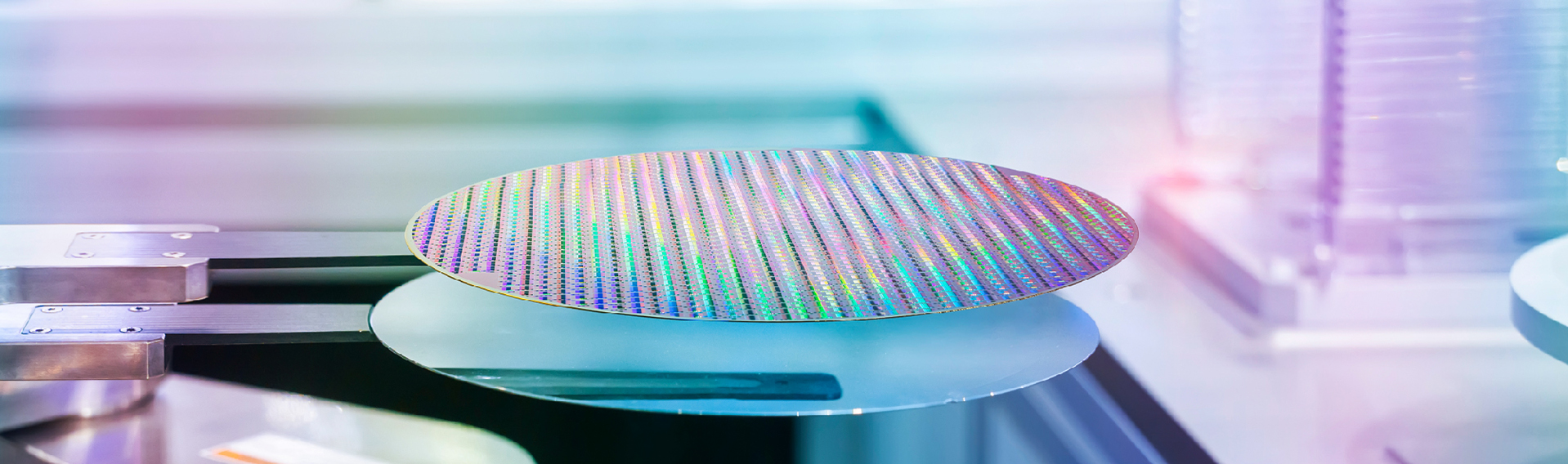
The expanding need for massive data storage and processing has driven the migration from 2D to 3D architectures for logic and memory chips. These complex architectures, with their high aspect ratio (HAR) designs and ultra-thin layers, are forcing advances in metal and oxide deposition processes. Atomic layer deposition (ALD) is usually the method of choice for producing uniform layers with precisely controlled composition.
Beyond being one of the fun words in the semiconductor industry, the “FOUP,” front-opening-unified-pod, represented a radical change that has influenced the productivity of each fab and contributed to the capabilities our electronic devices today. At the inception of Moore’s Law in 1965, 30 mm (1.25”) diameter wafers were the standard. Leading up to the late 1990’s, seven generations of incremental increases would be introduced. At each point, manufacturing efficiencies and device performance opportunities existed to get “Moore” out of each wafer. Wafer storage and transport was primarily accomplished in open-air cassettes and pods, leaving wafers more susceptible to physical damage and contamination.
Why Switch to our Bags? Supply chain issues? Breaking bags? Freezing problems? Our Aramus™ bags can get you back to making lifesaving therapeutics.
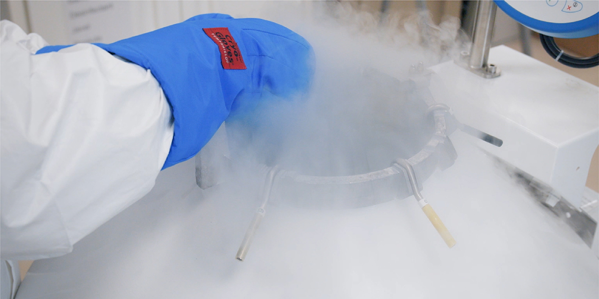
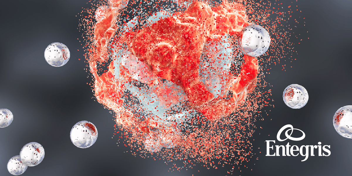
Freezing down bulk drug substance (BDS) isn’t something you can play around with. This is a high value product where any failure or contamination due to the bag breaking can lead to delays in medicine getting to the patient. Making sure you pick the right solution to protecting that product makes a big difference. Here are three questions you should be considering:
Since the introduction of the mobile phone, scientists and engineers have been on a series of quests to make them smaller and smarter. And incarnation after incarnation, from shoe box large to smart phone tiny, they succeeded. Until, that is, demand for more data, more storage, faster speeds, and longer battery life created major roadblocks. New smartphone capabilities — from biometrics to more accurate geopositioning, from artificial intelligence to virtual reality — demanded significant improvements in chip power. Their constant use required pronounced leaps in battery life.
The impact of the freeze/thaw process on workflows requires it be treated as a unit operation of its own.
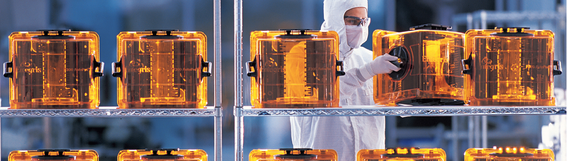
As a partner, Entegris is continuously developing solutions for our customers’ biggest challenges. An unprecedented pandemic came with a one-of-a-kind challenge: help a leading COVID-19 vaccine manufacturer scale up their process.
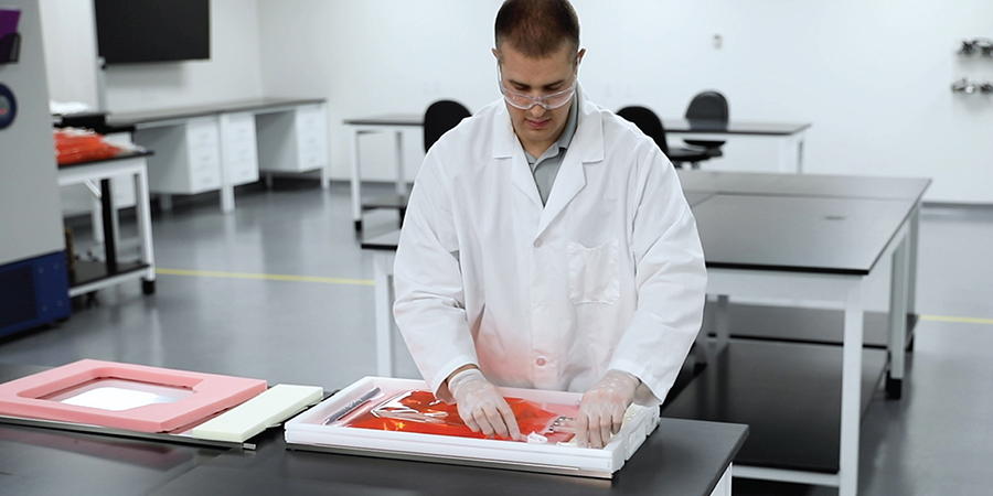
The pharmaceutical and biopharmaceutical industries continue to embrace the utilization of single-use systems (SUS). With the ever-growing adoption of SUS products, increasing scrutiny has been placed on the purity concerns of single-use components and their possible impact on the biomanufacturing, storage and transportation of high value final products.
Advanced 3D architectures for logic and memory devices increasingly rely on atomic layer deposition (ALD) to achieve high-quality, nanoscale conformal coatings. ALD deposits reactants and precursor molecules in alternating pulses to create the desired chemical makeup of the layers. Because of its ability to produce extremely thin films of uniform thickness and composition, ALD has supplanted physical vapor deposition (PVD) as the dominant deposition process for leading-edge technology nodes.
As a world-class supplier of advanced materials and process solutions for the semiconductor space, w...
Meet Regulatory Requirements to Ensure Patient Safety Developing and validating a robust freeze/thaw...

A major difference exists as more features from our smartphones are integrated, replicated, and expa...

The expanding need for massive data storage and processing has driven the migration from 2D to 3D ar...
Beyond being one of the fun words in the semiconductor industry, the “FOUP,” front-opening-unified-p...
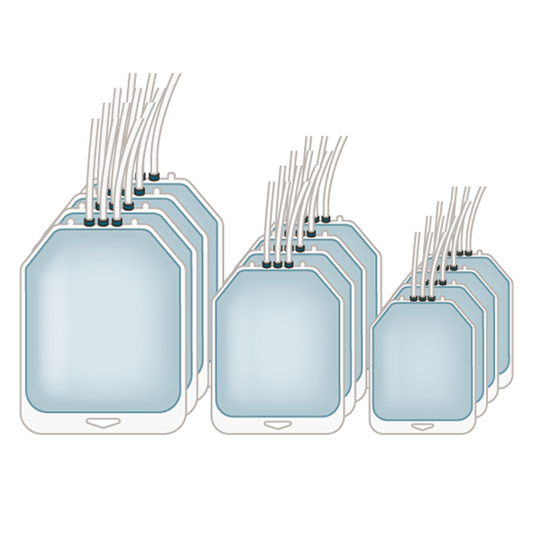
Why Switch to our Bags? Supply chain issues? Breaking bags? Freezing problems? Our Aramus™ bags can ...

Freezing down bulk drug substance (BDS) isn’t something you can play around with. This is a high val...
Since the introduction of the mobile phone, scientists and engineers have been on a series of quests...

The impact of the freeze/thaw process on workflows requires it be treated as a unit operation of its...

As a partner, Entegris is continuously developing solutions for our customers’ biggest challenges. A...
The pharmaceutical and biopharmaceutical industries continue to embrace the utilization of single-us...
Advanced 3D architectures for logic and memory devices increasingly rely on atomic layer deposition ...
© 2026 Entegris. All Rights Reserved

