A major difference exists as more features from our smartphones are integrated, replicated, and expanded in our cars - reliability expectations. A smartphone is designed to work effectively for 3-5 years while cars expect 10-15 years with standard maintenance. Failure in our cars can create dangerous situations for drivers, passengers, and others on the roadway. Designing and manufacturing our cars to ensure the functional safety along with the performance expectations of our new digital transportation systems is challenging manufacturing models for carmakers.
Table: A comparison of semiconductor customer requirements in different industries.4
| Semiconductor feature | Consumer electronics | Automotive electronics |
| Process node | 28 → 7 | 180 → 7 |
| Temperature range (ºF) | 32 to 100 | -40 to 300 |
| Operating lifetime (years) | 3 to 5 | 15 |
| Tolerated failure rate (per year) | <1,000 ppm | 0 ppb |
| Long-term supply needed | No | Yes, up to 30 years |
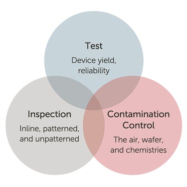
At the heart of the electronics that power and empower these electronic systems is the semiconductor, or “chip.” Each instruction the chip executes is dependent on the reliability of the chip, the integration of the package, and the coordination of the sub-systems in the software environment. The intersection of a semiconductor fab’s inspection, testing, and contamination control addresses the functional safety challenges the carmaker and their electronic supply chain faces. Each plays a vital role in the quality of the chip.
 Addressing functional safety where test,
inspection, and contamination intersect.
Today’s pattern inspection technology is incredibly powerful and provides invaluable insight into the process health in semiconductor manufacturing. There is a gap in the inspection capabilities though. Particle size sensitivities in liquids, gases, and ambient air are smaller than the identification capabilities of installed inspection tools in these applications. Other contaminants, such as metals, are also not visible in today’s inspection technology. What cannot be viewed is a threat to yield and reliability at this scale. To bridge this gap, advanced contamination control improves process performance, leading to improvements in wafer yield and device reliability. The relationship with yield and reliability are longstanding and form best practices in the management of raw materials throughout the supply chain journey.
|
"Inspection does not improve the quality, nor guarantee quality. Inspection is too late. The quality, − W. Edwards Deming, Out of the Crisis |
Implementing these best practices can be accomplished through a collaborative approach to compare contamination-control benchmarks to fab process areas such as photolithography, wet etch and clean, CMP, deposition, implant, or facility/sub-fab. Through comparison to established benchmarks, each process area identifies areas of concern that threaten yield and reliability performance. As we give up more control in our cars, the assurance of functional safety remains the same.
To learn more, read Entegris’ and Volkswagen’s white paper, “New Continuous Improvement Opportunities for Semiconductor Technologies Entering the Automotive Domain”.


