Hydrogen composes about 75% by mass of the normal matter in the universe, existing as H2 gas under standard conditions. This abundance of supply creates opportunities in numerous applications, including semiconductor manufacturing, for which hydrogen is considered a bulk gas and is employed in many parts of the ecosystem.

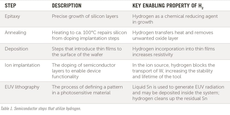
Key semiconductor steps in a fab that typically use hydrogen include:
- Epitaxy (precise growth of silicon layers) – H2 acts as a chemical reducing agent in layer growth;
- Annealing (repairing silicon from doping implantation via high heat) – H2 transfers heat and removes unwanted oxide layers;
- Deposition (placing thin films on the wafer surface) – H2 is incorporated into thin films to increase resistivity;
- Ion implantation (doping semiconductor layers to enable device functionality) – H2 blocks transport of tungsten in the ion source, increasing tool stability and lifetime; and
- EUV lithography (printing fine device patterns on a wafer) – H2 cleans up residual tin, which is used to generate EUV radiation and may be deposited inside the system.
With these processes comes the potential for contamination; ensuring the purity of H2 gas is critical to process yield. Surface science plays a major role in the purification of hydrogen. The surface-based technologies used to purify hydrogen for use in the manufacture of semiconductors include adsorption, cryogenics, and gettering.
Another important technique makes use of the element palladium (Pd). Because this metal is permeable to hydrogen but not to other atoms or molecules, palladium membranes are the only viable 100% selective purification technology for H2. By removing CH4, N2, and other persistent impurities from hydrogen process streams, the integrity of the wafer substrate can be maintained, reducing total cost of ownership and increasing yield.
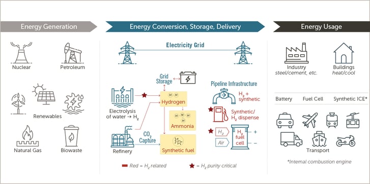
Tied to its importance to the semiconductor manufacturing process is hydrogen’s role in the transition to the new green-energy era. At the time of writing, the COP28 United Nations Climate Change Conference 2023 held in Dubai is ongoing and they note in their Declaration of Intent, second paragraph: Acknowledging that renewable and low-carbon hydrogen and hydrogen derivatives will play an essential role in meeting global energy needs and decarbonizing our industries as part of a people-centred energy transition to net zero that leaves no-one behind.
Producing hydrogen gas from water involves several steps. Generating H2 via electrolysis is a well-known process in which electricity is applied to water to separate the hydrogen and oxygen. Several electrolysis technologies (such as Alkaline, Polymer electrolyte and solid oxide) are in use today, each of which has pros and cons which determine suitability for the end use. The hydrogen produced through electrolysis has very high levels of moisture and, depending on the electrolysis technology, trace amounts of oxygen – both of which need to be removed before use in fuel cells, turbines, or other applications.
While hydrogen storage is an excellent match for renewable sources, which often generate power when it is least needed, challenges remain for preserving required H2 purity over time. Steam methane reforming (SMR) is an established technology in which the reaction of methane gas and steam produces hydrogen that is then cryogenically distilled for high-grade purification. Many hydrogen supplies are delivered and stored in the liquid phase, where purity can be maintained more easily.

Once the H2 is generated, it can be purified at the point of generation or at the point of use, depending on end use. For example, fuel cells, which convert hydrogen and oxygen from the air into electricity, are greatly impacted by high levels of contaminants.
Factors that affect this include manufacturing origin as well as the climate/environment and operating conditions in which the fuel cell will be used. Regardless of gas origin, however, hydrogen used in fuel cells must be purified at the point of dispense to guard against any additional unexpected impurities and ensure delivery of hydrogen at the required specification so that the cells aren’t damaged by any lingering contaminants.
The purification requirements for the semiconductor and energy sectors necessitate different technical approaches. However, these industries face similar challenges with regard to purification scale and cost of ownership. Through decades of development, Entegris’ brings deep knowledge of materials and gas purification to solve these challenges and ensure purity across the hydrogen landscape.
To learn more about hydrogen challenges for semiconductor manufacturing and the evolving energy ecosystem, read the article “Hydrogen Gas for Semiconductors and Clean Energy” in our 2022 Scientific Report.


