Gas Purifier Regeneration: Putting Circularity into Practice

Science that is transforming lives and enabling the future
Gas Purifier Regeneration: Putting Circularity into Practice
Changing one material in the semiconductor manufacturing process has a cascading effect on multiple process steps. Consider the replacement of tungsten (W) and copper (Cu) with molybdenum (Mo). Integrated device manufacturers (IDMs) are implementing Mo in advanced designs, focusing on 2-nanometer (nm) nodes and below. Mo is highly conductive, can be deposited without a titanium or titanium nitrid
Silicon carbide (SiC) has become popular with chipmakers. Its wide-bandgap structure offers many design benefits for the operations of power semiconductors. Compared to silicon, SiC wafers enable the fabrication of faster, more efficient devices that can both operate at higher temperatures and remain stable when deployed in extreme temperature environments. Processing SiC wafers using the same materials and methods as silicon wafers is not a viable option, however.
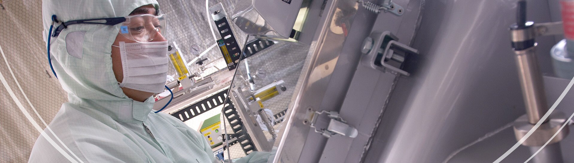
If you asked a semiconductor process engineer to name their biggest challenge when tackling the next technology node, they would likely tell you it is figuring out how to achieve high device yields. This is mainly due to an increase in possible points of contamination as the number of potential contaminants grows and their sizes shrink. It is becoming particularly difficult to detect metal contaminants and pinpoint their root cause so they can be eliminated. That’s because they can form anywhere in the process flow.
In the early days of semiconductor manufacturing, fabs would remove contaminants from their process fluids in a sequence that could be analogized to making a cup of coffee. By using a filter with tiny pores, large contaminants (coffee grounds) are separated from water. Because the coffee grounds are too large to pass through the filter, they can’t pass into the coffee we drink.
For decades, the semiconductor device manufacturing mantra was “How do we make them smaller, cheaper, and faster?” The pursuit of Moore’s Law – the doubling of transistors on a chip every two years – was achieved through planar scaling. But that approach could only go on for so long. The mantra now is “How do we improve power, performance, area, and cost (PPAC)?” At the 14 nm node, it was clear that the best way to push the limits of semiconductor device PPAC was to take it into the third dimension.
Whether it is a deliberate strategy or serendipity, the innovations that shape our lives are the result of skilled people put into the right environment to create something new. Innovation is not an exact science, but persistence and some good luck have yielded all the amazing tools and technology we rely upon.
The expanding need for massive data storage and processing has driven the migration from 2D to 3D architectures for logic and memory chips. These complex architectures, with their high aspect ratio (HAR) designs and ultra-thin layers, are forcing advances in metal and oxide deposition processes. Atomic layer deposition (ALD) is usually the method of choice for producing uniform layers with precisely controlled composition.
Advanced 3D architectures for logic and memory devices increasingly rely on atomic layer deposition (ALD) to achieve high-quality, nanoscale conformal coatings. ALD deposits reactants and precursor molecules in alternating pulses to create the desired chemical makeup of the layers. Because of its ability to produce extremely thin films of uniform thickness and composition, ALD has supplanted physical vapor deposition (PVD) as the dominant deposition process for leading-edge technology nodes.
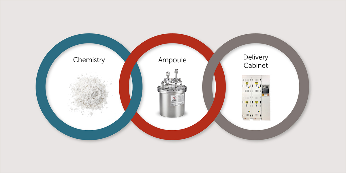
The Entegris Safe Delivery Source® (SDS®) package has been the leader in providing subatmospheric specialty gas storage and delivery for ion implant dopant materials since its inception more than twenty years ago.
The purpose of a CMP process is simple – to planarize the top layer of oxide or metal with an abrasive slurry. Manufacturing the slurry to the exacting standards required by the end user is not easy. To effectively planarize the wafer surfaces, both large and small abrasive particles must be removed prior to being dispensed. Thus, the target is a narrow particle size distribution between 30 and 200 nm to prevent both microscratches and underlayer defects.
Simplify your operations and supply chain with a versatile contamination control strategy.
Gas Purifier Regeneration: Putting Circularity into Practice
Changing one material in the semiconductor manufacturing process has a cascading effect on multiple ...

Silicon carbide (SiC) has become popular with chipmakers. Its wide-bandgap structure offers many des...

If you asked a semiconductor process engineer to name their biggest challenge when tackling the next...

In the early days of semiconductor manufacturing, fabs would remove contaminants from their process ...

For decades, the semiconductor device manufacturing mantra was “How do we make them smaller, cheaper...

Whether it is a deliberate strategy or serendipity, the innovations that shape our lives are the res...

The expanding need for massive data storage and processing has driven the migration from 2D to 3D ar...
Advanced 3D architectures for logic and memory devices increasingly rely on atomic layer deposition ...

The Entegris Safe Delivery Source® (SDS®) package has been the leader in providing subatmospheric sp...
The purpose of a CMP process is simple – to planarize the top layer of oxide or metal with an abrasi...

Simplify your operations and supply chain with a versatile contamination control strategy.
© 2026 Entegris. All Rights Reserved

