The expanding need for massive data storage and processing has driven the migration from 2D to 3D architectures for logic and memory chips. These complex architectures, with their high aspect ratio (HAR) designs and ultra-thin layers, are forcing advances in metal and oxide deposition processes. Atomic layer deposition (ALD) is usually the method of choice for producing uniform layers with precisely controlled composition.
ALD precursor delivery systems were originally developed for materials that arrived at the fab in gaseous form. For precursors that are gases at standard temperature and pressure, the process is well-established. Precursor gases flow directly into the deposition chamber.
Many of the precursor materials needed for the most advanced devices, however, are only available as solid powders. Most of these materials sublimate rather than melt as they are heated. These powders are stored as solids and sublimed in the ALD tool so their vapor can be delivered to the wafer. The gas lines delivering the precursor must be heated as well to prevent condensation of solids.
Solid Precursor Delivery

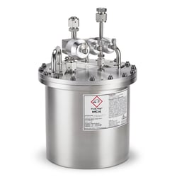
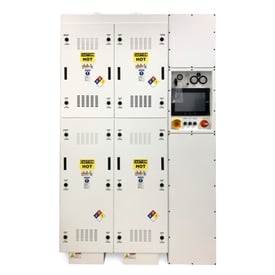
Solid precursors are often shipped in ampoules—vessels from which the precursor vapor can be delivered directly to the ALD tool. A properly configured delivery system improves efficiency. For example, a system consisting of two ampoules inside a custom cabinet allows for continuous operation. When one ampoule empties, the system automatically switches to the other vessel to keep the process running.
Temperature control is critical. An optimized process will consume at least 90% of the precursor in each ampoule to minimize waste and improve cost-of-ownership. The precursor must be heated just enough to fully vaporize it for deposition onto the wafer. Too high a temperature, and the precursor may decompose. If the temperature is too low, the vapor flow to the process is insufficient.
Commercial ALD tools have a built-in heating capability for vaporizing solid precursors, and temperature control is not terribly difficult. But that alone is not enough to enable reliable solid precursor processing. Additional steps are necessary to ensure consistent delivery of high-purity materials to the wafer.
Protective Coatings
The combination of reactive chemicals and elevated temperatures creates a corrosive environment that will degrade any metal components exposed to the precursor. Such degradation compromises the components’ integrity, but that is not the only concern. Particles that shed from components can contaminate the precursor. Contaminants that reach the deposition chamber can create defects on the wafer, reducing yield.
Protective coatings are recommended for any exposed metal components. These coatings mitigate contamination by forming a diffusion barrier that keeps the metal surface from reacting with the precursor. Various coating materials are available to ensure compatibility with different precursors and substrates.
Ideal coatings are inert compounds that adhere well to the substrate surface and do not react with the precursor. Potential coating materials include a variety of transition metal or rare earth oxides, plus some fluorides and nitrides. Working with a vendor that supplies precursor materials, protective coatings, and system components streamlines the coating selection process.
Coatings should be applied to the inside surfaces of all components in the delivery system including ampoules, ampoule lids, trays, valves, filters, and gas lines. The trays inside the ampoule are especially critical because they are in direct and constant contact with the precursor.
 Gas lines face different risks. Chemical exposure is intermittent rather than constant, but gas lines are exposed to the atmosphere whenever the delivery system is serviced. Moisture can enter the lines and increase the risk of oxidation. For this reason, a protective coating is essential.
Coatings eventually wear out, often while a component is otherwise in excellent condition. Component refurbishing—stripping the damaged coating and reapplying a fresh coating—extends the lifetime of the trays and other components. Refurbishing is a proven way to improve cost of ownership of the solid precursor delivery system.
While protective coatings can be applied using any conventional deposition process, ALD is ideal because it creates dense, highly conformal coatings. Several components in the precursor delivery system feature complex shapes or HAR geometries, both of which benefit from the conformal nature of ALD.
The density of ALD coatings allows them to be thinner than coatings applied using other techniques while providing thorough coverage. Thinner coatings are advantageous because they use less material and promote better temperature stability. The precise coating thickness—typically in the sub-micron range—can be tailored to the application.
Equipment is a critical part of the precursor delivery process, but device performance depends highly on the quality of the starting material.
For more details see the white paper, “Solid Precursors for 3D Architectures: Materials, Processing, and Delivery,” on how new precursor materials, in conjunction with optimized delivery systems, are enabling the next generation of advanced logic and memory chips.
Also, read our related blog on how to avoid defects using solid precursors and delivery systems.


