

Beyond being one of the fun words in the semiconductor industry, the “FOUP,” front-opening-unified-pod, represented a radical change that has influenced the productivity of each fab and contributed to the capabilities our electronic devices today. At the inception of Moore’s Law in 1965, 30 mm (1.25”) diameter wafers were the standard. Leading up to the late 1990’s, seven generations of incremental increases would be introduced. At each point, manufacturing efficiencies and device performance opportunities existed to get “Moore” out of each wafer. Wafer storage and transport was primarily accomplished in open-air cassettes and pods, leaving wafers more susceptible to physical damage and contamination.
During the early days of the transition from 200 to 300 mm wafers, all aspects of wafer protection had escalated to critical concerns as chip complexity rose and fabs continued to seek process improvements. A small start-up proposed a new wafer handling approach and climbed the mountain of tasks with partners to introduce what is today the standard wafer transport solution around the world for 300 mm fabs (~120 and growing), the FOUP.
The story is best told by Gary Gallagher, senior director and “Father of the FOUP.” Much like other innovation stories, there were early adopters that proved instrumental in shaking up the traditional view from the top. There are also some twists along the way that make for another great story of how semiconductors continue to influence our lives because of the pioneers and partnerships that come with asking, “what if we ______?”.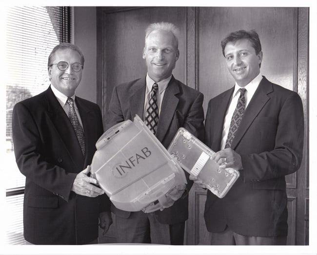
Figure 1. “Father of the FOUP,” Gary Gallagher (center), as part of the original pioneers responsible for revolutionizing wafer handling technology.

Figure 2. Clint Haris, current Entegris SVP & GM
Microcontamination Control Division, as "the young
Motorola engineer" assigned to implement the first
high-volume manufactured FOUPs.
Learn more about how Entegris provides full container solutions to monitor, protect, transport, and deliver wafers from the front-end through to the back-end of the fab.

