Advanced 3D architectures for logic and memory devices increasingly rely on atomic layer deposition (ALD) to achieve high-quality, nanoscale conformal coatings. ALD deposits reactants and precursor molecules in alternating pulses to create the desired chemical makeup of the layers. Because of its ability to produce extremely thin films of uniform thickness and composition, ALD has supplanted physical vapor deposition (PVD) as the dominant deposition process for leading-edge technology nodes.
ALD is a mature process. When working with precursors that are gases at standard temperature and pressure, the precursors flow directly into the deposition chamber ready to deliver to the wafer. Not all precursors, however, are available in gaseous form.
Liquid and Solid Precursor Materials
Today’s most advanced chips require a greater variety of both device materials and interconnect materials. Many of the precursors needed to deposit these metals are liquids or solids at room temperature. The vapor pressure of the precursors determines the process conditions required to vaporize them for delivery to the wafer.
Some liquid precursors are delivered at room temperature and vaporized by lowering the pressure. Many integrated device manufacturers (IDMs) prefer working with liquids because they are easier to transport around the fab.
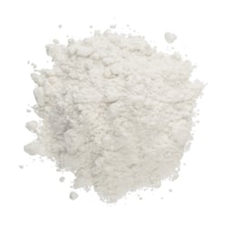
Solids are more challenging than liquids because of the need to heat the materials and the gas lines delivering them. Most solid precursors start as powders, which sublime into vapors for delivery to the wafer. Many of these materials are flammable or corrosive, which further complicates handling.
Solid precursors based on hafnium and zirconium have been used in semiconductor fabs for decades. New solid precursors based on aluminum (Al), molybdenum (Mo), and tungsten (W) are needed to meet the device and integration requirements for the latest generation of 3D devices. As layers become thinner, materials requirements often change.
The drive toward fluorine-free materials mitigates yield loss that can occur when fluorine reacts with nanoscale layers in devices. In the case of W precursors, tungsten pentachloride (WCl5) is replacing gaseous tungsten hexafluoride (WF6). WCl5 is a solid at room temperature.
Design constraints are not the only concern. For Al2O3 deposition, the conventional liquid precursors such as trimethyl aluminum (TMA) are extremely volatile and spontaneously ignite when exposed to air. Solid materials like AlCl3 provide a safer alternative.
Scaling Production
Fabs are accustomed to delivering gas and liquid precursors in high-volume production but has only been done for a few cases for solid precursors. Successful scaling requires precise and repeatable control over the precursor mass flow rate and chemical purity.
As a solid is heated, its vapor pressure increases, and the equipment must be adjusted to maintain the target precursor delivery rate. Unlike with gases, it is not possible to install pressure regulators at the point of delivery to adjust the pressure in situ. Mass flow rate testing ensures that the pressure remains steady as the precursor flows from the storage ampule to the ALD chamber.
Production should start with high-purity powders. If commercially available powders are not available at the required purity, it is best to work with a precursor supplier that can start from scratch and synthesize a custom-made, contamination-free formulation.
Choosing a precursor material supplier with in-house purification and synthesis capabilities greatly reduces the risk of contamination. The chosen supplier should provide a certificate of analysis that will give fabs confidence about the chemical composition and purity of the precursors.
Temperature control is also important during both storage and delivery. While the precursor remains stable during storage at room temperature, it must be heated at just the right rate for delivery to the ALD chamber. The temperature must be high enough to fully vaporize the precursor but not so high that it causes excess material delivery or precursor decomposition.
The introduction of solid precursors complicates deposition processes, but solutions are available. By starting with high-purity powders, choosing the right equipment, and using comprehensive analytical data to adjust process conditions, IDMs can successfully incorporate solid precursors into their process flow.
For more details see the white paper, “Solid Precursors for 3D Architectures: Materials, Processing, and Delivery,” on how advances in materials, processing, and delivery are enabling the next generation of advanced logic and memory chips.
Also, read our related blog on how to avoid defects using solid precursors and delivery systems.


