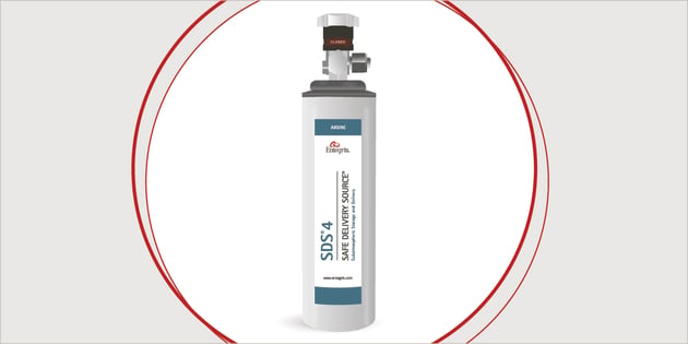
The Entegris Safe Delivery Source® (SDS®) package has been the leader in providing subatmospheric specialty gas storage and delivery for ion implant dopant materials since its inception more than twenty years ago.
As semiconductor devices advance, increased demands are placed on the purity, productivity, and safety of electronic gases. SDS4, the fourth generation of the SDS product line is designed to address these increasingly stringent demands.
 In our paper, “Next Generation Safe Delivery Source® (SDS®4) Dopant Material Storage and Delivery Package” we present key advancements in adsorbent-based packages for storing, handling, and delivering semiconductor dopant gases. Desirable characteristics and properties of adsorbents for use in this application are reviewed. The screening methodology and performance of various carbon and metal organic framework (MOF) adsorbents are evaluated against these characteristics.
Further discussion is included on the testing, design, and selection of cylinder features to continuously improve the SDS product line, making SDS4 the safest and highest performing sub-atmospheric storage and delivery package to- date. Final product performance is demonstrated and verified through beamline ion implantation tool data.
To read the full paper, visit Entegris website: Next Generation Safe Delivery Source® (SDS®4) Dopant Material Storage and Delivery Package
Authors: Christopher Scannell, Joseph Despres, Edward Sturm, Kavita Murthi, Oleg Byl – Entegris


