Like all reticles, those used for EUV lithography rely on reticle pods for safe storage and to protect them during lithographic patterning, inspection, cleaning, and repair.
All surfaces that contact or surround a reticle, including those of the pod, must remain ultraclean to avoid introducing contamination in the form of particles or airborne chemical vapors. The finer the lithographic patterns, the greater the risk reticle contamination poses. Potential contamination sources include both foreign particles and chemical residues. Reticle coatings are very delicate and easily damaged. Anything that touches a reticle, whether it is an expected part of the process such as a robot arm in the fab or an unexpected contaminant such as a human hair, has the potential to cause damage.
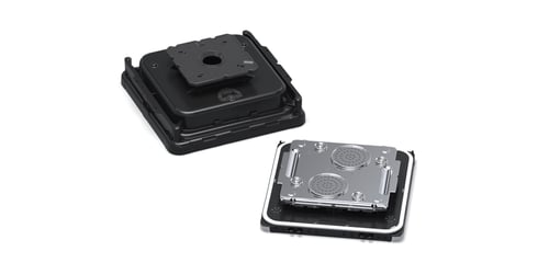
Today, the dual-pod configuration is standard practice for EUV lithography, and such pods are commercially available. Just because they are readily available, however, does not mean that they are a commodity product. EUV pod designs, Figure 1, continue to evolve to meet demands for performance and lithography throughput.
Figure 1. Dual-pod configuration for EUV lithography showing outer pod (left) and inner pod (right).

Despite the protection that the dual-pod configuration conveys, the potential for contamination is significant. For this reason, EUV pods must be developed with contamination risk mitigation in mind. Especially for reticles that do not include a pellicle, the inner pod is the primary source of both protection and potential contamination.
Pod design considerations cover both the geometry of the inner and outer pods and the materials from which they are made, including:
- Material cleanliness
- Ensuring mechanical protection
- Purging the pod
- Equipment compatibility
- Accommodating pellicles
Because reticle pods are intended to last many years, they must meet the needs of current and future EUV lithography. Polymers that outgas create undesirable chemical contamination that can deposit on the reticle surface. Pod material should, therefore, be chosen to minimize the potential for outgassing.
Regular purging of the outer pod is required to remove moisture inside and maintain a clean, dry environment for the reticle. In an ideal design, the filter conductance — a measure of the ability for air to flow through the filter — should be much greater than the seal conductance, so that at least 90% of the air entering the inner pod enters through the filters.
Much of the lithographic process is automated and the expected long lifetime of pods means that they will experience thousands of open/close cycles over many years. Using materials that resist wear both minimizes particle contamination and extends the useful life of the pods.
Today’s pod designers should also consider a version that includes space to accommodate a pellicle as well as a version for use without a pellicle. Designing a pellicle-compatible pod requires close collaboration between the pod manufacturer, pellicle supplier, and lithography tool manufacturer.
EUV reticle pods are highly specialized pieces of equipment that fulfill a critical role in EUV lithography. They must protect the reticle during use, storage, and transportation while not introducing additional contamination or damage. Pods must be compatible with lithography equipment and be able to maintain a clean, dry atmosphere for the reticle. Precisely designed dual-pod configurations achieve these goals for reticles both with and without pellicles, ensuring the future of EUV lithography.
For further information download the white paper, Enabling Advanced Lithography: The Challenges of Storing and Transporting EUV Reticles


