hero-654791312-sized

Ensights

Science that is transforming lives and enabling the future

Case Study: On-Wafer Defect Reduction in Lithography

All Posts

Case Study: On-Wafer Defect Reduction in Lithography

Overview

The rapid increase of semiconductors in cars enables significant safety, connectivity, mobility, and sustainability improvements. As transportation transforms from being driver controlled to software controlled, automakers must look closer at their ability to measure and maintain product reliability throughout the vehicle’s lifetime.

In today’s microelectronics manufacturing facilities, Advanced Fault Detection Classification (FDC) is required even more to guarantee quality in terms of process stability, defect reduction, and tighter uniformity.

In collaboration with STMicroelectronics, this case study looks at how to effectively collect data to improve your process control strategy and lower defectivity.

Customer Issue

Our customer’s resist dispense pump installed base was old and aging. Filtration was not always under control and thus negatively affecting dispense repeatability and stability. In addition, they were looking for a way to collect detailed dispense line status data to improve their photolithography process.

Approach IntelliGen_ULV-3150-1215
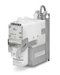
We proposed they evaluate our IntelliGen® LV two-stage technology dispense system that offers:

1.  independent filtration and dispense functionality

2.  dispense monitoring and confirmation capabilities


Two-Stage Dispense Technology

ENTG-dispense-technology-fig-1-2

Figure 1: During filtration (idle times between dispenses), the dispense pump's motor reverses
direction and the feed pump pushes the fluid slowly through the filter at the programmed rate (typically
0.1 to 0.5 mL/sec).
Figure 2: During dispense, the filter is isolated from
the dispense chamber to minimize pressure changes
that affect repeatability. Typical dispense rates are between 1 and 2 mL/sec.


Read the full case study
to better understand the difference with a single-stage pump technology and know more about the dispense monitoring and confirmation capabilities.

Results

Thanks to Entegris’ solution, STMicroelectronics achieved

  • Three times lower wafer defectivity
  • 30% tighter wafer dispense uniformity
  • Stability over six months of operation

Download the full case study to see the experiment design and illustrations of the results.


ConclusionSTMicroelectronics

According to STMicroelectronics, the IntelliGen dispense pump from Entegris is one of the best pump resist systems. It enabled guaranteed process stability, thickness uniformity, defectivity reduction, and statistical process control (SPC.) The network communication capability allowed data collection and storage in fab management systems. All these features combined to greatly improve the process quality and significantly reduce wafer excursions.

For more information on this solution, please visit the IntelliGen LV Dispense Systems product page.


Related Posts

Exploring the Superiority of Silicon Carbide in Optical Components

Exploring the Superiority of Silicon Carbide in Optical Components Silicon carbide (SiC) is a leading material for high-performance optical components, offering numerous advantages over traditional materials such as glass and metal. Its exceptional specific stiffness, high thermal conductivity, and outstanding dimensional stability position SiC as a superior choice compared to beryllium and low-expansion glass ceramics. Historically, the high costs associated with the preliminary shaping and final finishing of SiC have hindered its widespread adoption in optical systems. The material is both hard and strong, requiring precision machining with expensive diamond tooling on high-quality, rigid machine tools. However, advances in manufacturing techniques, such as near-net-shape slip casting, have demonstrated success in reducing costs despite necessitating significant diamond grinding. Building on this success, Entegris offers an entirely new way of creating SiC. Using our chemical vapor conversion process, we can create net- or near net-shaped SiC components in complex forms while spending much less time on fabrication.

Entegris Offers New FOUP Form-Factors for Non-Standard Wafers

Entegris Offers New FOUP Form-Factors for Non-Standard Wafers Over the last few years, 3D stacking has gone from a relatively niche fabrication method to an absolute necessity for cutting-edge applications. As chipmakers delve into smaller and smaller nodes, stacking and die-bonding wafers has become a preferred way of creating more processing power in a smaller space. Stacked and bonded wafers don’t behave the same way as 2D wafers: Wafers are thinned prior to bonding, which results in wafers that can sag when handled Bonded wafers are thicker and heavier than 2D wafers when assembled Bonded wafers can also warp following assembly Many automation tools rely on the predictable geometry and characteristics of 2D silicon wafers for safe handling and transport. While stacked and bonded wafers are a game-changer for miniaturization, they can also force manufacturing compromises unless chipmakers adopt specialized tools for the back end of the line (BEOL).

Mastering the SiC Wafer Transition

The use of silicon carbide (SiC) semiconductors offers a huge advantage for electric vehicles (EVs) due to lower switching losses and higher efficiencies, but cost has always been a drawback. SiC wafer manufacturing can suffer from high costs and lower yields, causing SiC semiconductors to cost up to eight times more than their silicon equivalents. This cost often gets passed on to the end customer, making EVs more expensive.