

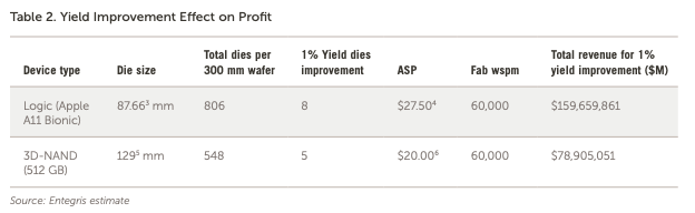
One of the longest held beliefs in semiconductor manufacturing is that yield is the single most important factor in overall wafer processing costs. Even incremental yield increases can significantly reduce manufacturing cost per wafer, or cost per square centimeter of silicon. As such, yield improvement is critical to any successful semiconductor operation. As semiconductor device nodes continue to scale, and
7 nm lines are ramping to production, this belief continues to ring true.
Today’s fine geometries and vertical structures, such as FinFET logic devices and 3D NAND flash memory, are even more prone to yield hits due to process variability and contamination. These risks are tied not only to device design, but the equipment and processes being used to manufacture them. For example, an excursion – that is, when a process or piece of equipment moves out of preset specifications – can be a significant contributor to yield loss, particularly if it goes undiscovered until after fabrication. Therefore, steps that assure wafer defect reduction are critical to yield management.
Over 20 years ago, the semiconductor manufacturing industry moved to factory automation, not only to increase device throughput, but also to mitigate yield risk caused by human interaction with wafers. Wafer transport and handling systems became an essential part of the manufacturing process flow to maintain a clean environment for the wafers. These systems comprise three types of wafer handling carriers: Front opening shipping boxes (FOSB) for transporting from the wafer supplier to the fab; front opening unified pods (FOUPs) for transport within the fab; and horizontal wafer shippers (HWS) for transport to final assembly. This paper focuses specially on FOUPs, and how yield advantages can be achieved simply through proper maintenance and upgrades of your FOUP fleet.
A FOUP’s Journey
FOUPs were originally designed to serve as a wafer transport carrier from the FOSB, and then from process chamber to process chamber. They had shock-absorbing capabilities, humidity control, and were designed to minimize particle contamination. As technology nodes continued to shrink past 10 nm to 7 nm development, the industry needed modified FOUP capabilities to keep these delicate and costly wafers safe. Some of these modifications included a change in FOUP materials for the shells, gaskets, and valves. Advanced purge capabilities were also necessary for 7 nm node processes and beyond to prevent contamination during copper etch processes.
As a result, today’s FOUPs not only address particles, but also minimize and control volatile organic compounds (VOCs), oxygen, and relative humidity. Any of these potential contamination sources can negatively impact device yield.3 In fact, FOUPs are one of the most important devices a fab has, because they provide a hyper-clean microenvironment for the wafers they are protecting.
These FOUPs offer a sealed wafer environment that provides static protection, white-light shielding, and control moisture and oxygen. The purge ports make it possible to fill the FOUP with nitrogen during processing and storage. Advanced purge capabilities allow for uniform airflow across the wafer surface by bringing air from the bottom of the box and along the vertical access. In this way, the wafers are bathed in nitrogen as they are processing into and out of the FOUP, keeping oxygen and moisture concentrations low. This prevents the opportunity for excessive etching or corrosion.4 This is important because as wafers exit a process, residual gas or other materials may remain on the surface that may continue to outgas. If these are not removed from the wafer surface, they will continue to react inside the FOUP, and can result in defects forming on the wafer.
A wafer will travel 8 to 16 km within the fab as it moves through the process steps required to manufacture each microchip. In advanced microprocessor manufacturing, there can be up to 400 steps with the FOUP docking at between 100 and 200 process tools, and with door open periods of up to 30 minutes. Each step creates a significant risk for yield-impacting contamination. As such, without careful maintenance, FOUP fleets begin to show the effects such as broken or improperly installed wafer retainers, cassettes, and filter assemblies; pinched or deformed door gaskets; shell scratches or cracks; cracked or damaged door housing; contamination from metal, chemicals, broken wafers, and process issues, such as post-etch copper contamination, Figure 1.
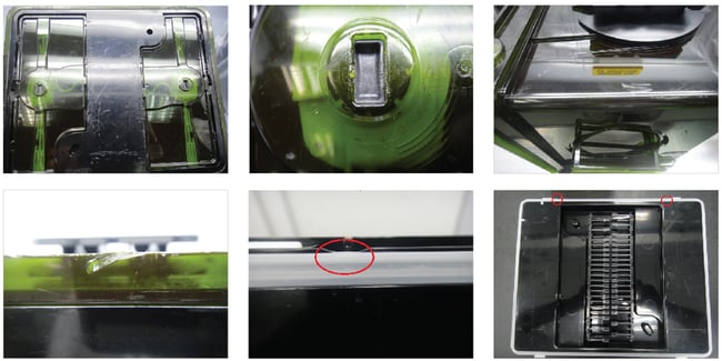
Figure 1. Aesthetic issues on aging FOUPs include (Top to bottom, L-R): scratched doors, dented door at load
port key interface, top shell scratches, top shell dents, gasket area dents, deformation on gaskets.
STEPS FOR PROPER FOUP MAINTENANCE
Analysis shows that after several years of use, FOUPs begin to show signs of degradation and general wear. Gaskets and O-rings become deformed, filters and components are damaged, and microcracks caused by accidental mishandling begin to appear. Additionally, dimensions can move out of specification. This significantly impacts FOUP cleanliness and proper function.
Routinely washing a FOUP will remove many surface particles, but there are still chances that particles or other forms of contamination get by a deformed gasket, O-ring, filter, or damaged component. That is why a regular FOUP maintenance program is critical for ensuring that the FOUP environment is consistently and constantly clean.
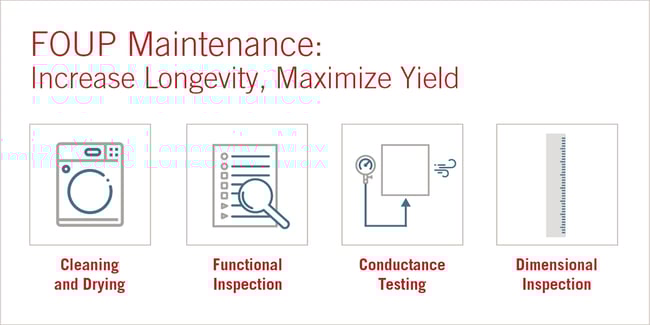
It is helpful for semiconductor manufacturing companies to have either a dedicated area in which to perform regular and systematic FOUP maintenance, or contract with a service provider for this task. Table 1 describes FOUP maintenance steps in more detail, including frequency, to make sure a FOUP is properly maintained.
In parallel to the regular maintenance program described here, FOUPs that have experienced excursions on the production floor should also be evaluated. These excursions could include a fall from the load port, being hit during the automation process, increases in chemical deviation from the wafers, etc. They are examined for broken doors, diffusers, and seals and repaired if possible. Companies that follow this maintenance protocol have reported that after 13 years of use, FOUP fleets are still being used successfully.
| PREVENTATIVE MAINTENANCE | FREQUENCY | ACTION |
| Visual inspection | Prior to every cleaning | Visually inspect the FOUP for damage and excessive wear and tear. Replace any worn or damaged components. |
| Functional inspection | Prior to every cleaning | Check the function and torque of the door’s latching system to make sure that it is functioning per the FOUP manufactures recommendations. |
| Dimensional inspection | Every three months; and when a failure is identified in the visual or functional inspection, or after a tool interface failure. | Inspect the FOUPs door dimensions and the shells front flange position, registration, and key slots and wafer positions to ensure that they are within specifications. |
Download the full paper to discover the five other steps.
FOUP REFURBISHMENT SAVES COMPANIES $1.2 - 2M
Every manufacturing facility with 7 nm production lines is now running FOUP fleets outfitted with the latest technologies. Facilities currently running legacy node lines, such as 65 nm and 45 nm, that ramp to more advanced nodes will benefit from utilizing the new technologies and designs of these more advanced FOUP platforms. However, replacing an entire FOUP fleet can be a multimillion-dollar expense and outside available budgets. Fortunately, there are retrofit solutions for certain situations.
That said, investing in a new fleet does have key advantages. The latest FOUP platforms enable upgradeable features so fabs can decide which technologies to invest in now, and which can be retrofitted later. Studies show that companies who invest in upgrading their FOUP fleet with purge and other leading technologies achieve upwards of three die-per-wafer increases.
Conclusion
It is well understood that yield management is critical to semiconductor manufacturing success. If yields are dropping, FOUP maintenance or upgrades may be beneficial. Many fabs ignore FOUP maintenance, not realizing the impact it can have on final yields, and as a result, the bottom line. While FOUPs will degrade over time, full replacement of a fab’s FOUP fleet is a costly endeavor. It is important, therefore, for every semiconductor manufacturer to evaluate their FOUP maintenance protocol and determine if improvements should be made.
To read the full paper visit www.entegris.com/foup

