A high purity sub-fab serves as the central nervous system of a semiconductor cleanroom. It houses chemical delivery, purification, recycling, and destruction systems. The sub-fab is where potentially hazardous aqueous chemistries and gases are stored and handled until they are delivered to the cleanroom process equipment located either in the floor above it or the building adjacent to it.
To mitigate any potential disasters, sub-fab plumbing must be designed using a dual containment system to prevent chemical contamination if the primary tubing leaks or ruptures. The secondary pipe acts as a catch basin that directs the chemistry to a known drain. Conventional approaches to dual containment rely on threading a single-wall tubing constructed from perfluoroalkoxy (PFA) tubing through clear, rigid polyvinyl chloride (PVC) pipe.
This PFA/PVC approach is not only outdated, it is susceptible to a myriad of pitfalls. Considering the current demand for computer chips that is driving a surge in new fab construction as well as existing fab expansion, now is the time to consider alternative approaches that will save time and money and deliver an improved outcome.
The Pitfalls of PVC Containment Pipe
It takes many miles of high-purity tubing—routed around gas cabinets, communication trays and channels, large HVAC plumbing and ducting systems—to support process chemistry plumbing between the sub-fab and the cleanroom.
High-purity PFA tubing is the ideal selection for the primary tubing in sub-fab dual containment systems because it is extremely chemically inert, ultraclean, and can be extruded in long lengths. However, because unlike PFA, PVC is subject to chemical degradation, using it as the outer containment can lead to the degradation of the PVC itself due to the fume-laden gas created between the outside of the PFA tubing and inside the PVC pipe.
Additionally, because PVC is rigid, it does not bend easily around structures in its path and requires custom bending. Long pipe runs are difficult to thread PFA through, which increases the risk of damaging the primary tube. These combined challenges create rigid plumbing that takes several days to install.
High-Purity PFA Tubing Is the Answer
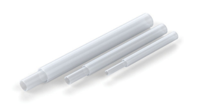
Tube-within-a-tube dual containment tubing (DCT) provides a flexible and cost-effective alternative to conventional, rigid PFA/PVC systems for high-purity sub-fabs in new greenfield fab construction, capacity expansions, and equipment upgrades, Figure 1A.

Figure 1. Tube-within-a-tube DCT offers a cleaner alternative to PFA/PVC systems.
By co-extruding a special-blend PFA outer tube around the primary containment tube, it is possible to create a dual containment system in which one tube floats inside the other, leaving annular space around the primary tube. There is no need to pull one tube through the other, reducing installation complexity as well as reducing the potential for contamination or damage.
DCT installs easily in areas that are densely populated with other facility plumbing or infrastructure where it is difficult to route rigid PVC containment pipe. It is available in long, continuous lengths that can flex around tight corners. Because it is self-contained on large reels that pay out a continuous feed, the tubing can be rapidly routed from the starting point, throughout the facility and around existing infrastructure. The result is a safe, reliable DCT system that can be installed or retrofitted in mere hours instead of days.
Conclusion
A dual containment system built entirely from flexible, PFA tubing creates an ultra-clean environment that is free from degradation and less affected by temperature changes. Ease-of installation makes it cost effective. It is therefore the ideal solution for high-purity sub-fabs.
To learn more about why now is a good time to consider a tube-within-a-tube DCT solution, and how it can solve sub-fab process plumbing challenges, read our white paper here.


