

The explosion of data generation has been accompanied by a corresponding explosion of memory storage technology options. The array of acronyms is astounding—NAND, DRAM, SRAM, MRAM, PCRAM—and finding the right option
can be complicated. For applications that need nonvolatile memory with high switching speed and fast data access, storage class memory (SCM) can be a
perfect fit.
SCM sits in the middle of the memory hierarchy and fills a vital performance gap.
The typical SCM space spans access speeds from 50 nanoseconds (ns) to 600 microseconds. SCM is also nonvolatile, avoiding the constant refresh required for DRAM, thus, saving energy.
The SCM category encompasses several technologies, including phase change memory (PCM) alloys. Some of these PCM alloys have especially fast switching speeds, allowing PCM-based memory devices (PCRAM) to achieve access speeds
of less than 20 ns, overlapping with DRAM.
 Although SCM is an excellent solution, increasing the memory density for demanding applications can be tricky. Shrinking the cell size to increase density is impossible beyond a certain point because cell-to-cell thermal disturbances limit the cell pitch.
As noted in the first blog in the series, the tiger is revered as a ferocious hunter,
but is also inefficient (chase to catch ratio of 5%). As it matures with hunting experience, the tiger realizes it does no good to keep hunting in an area once the prey has scattered. The tiger needs to head off in a different direction to ensure its own sustainability. Regarding SCM design, we benefit from thinking vertically rather than horizontally. The answer to the density challenge lies in novel stacked 2D or 3D device architectures. With all novel technology, the yield ramp can be steep.
One configuration for a PCRAM cell sandwiches a layer of PCM and a selector device between two metal electrodes. The selector isolates the cell and provides input current for switching. An optimum cell design keeps the cross-sectional area low, thermally insulates the cell for more efficient heating, and tailors the PCM composition. All of these factors minimize the reset current, allowing for lower power consumption per cell so that more memory cells can be switched on at once without overloading the circuit.
Stacking two planar PCRAM cell arrays creates a 3D structure. This structure is used to make the 3D cross-point device, a commercial PCRAM product, and is considered state-of-the-art technology. It exhibits higher density than DRAM devices, with a reported switching speed 1000 times faster than NAND and endurance 100 to 10,000 times than that of NAND.
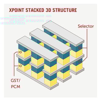
What if we could extend this stacking concept and stack multiple arrays of cells vertically? That seems like a simple way to increase memory storage capacity, but implementing it is far from simple. The 3D cross-point device is built sequentially layer by layer. Each layer requires lithography, etching, and sputtering. Stacking many layers in this manner would be extremely time-consuming and cost prohibitive. Overwhelmed with a similar complexity, the tiger may freeze and lose out on the prey.
We need to venture into somewhat unexplored territory. A true 3D structure would optimize the cost/performance tradeoffs and address the cost-of-ownership (CoO) gap if all layers could be manufactured in parallel. Vertical channels filled with PCM would create chains of cells in the vertical direction to enable higher-density PCRAM while reducing the number of processing steps. This approach creates the critical vertical structure in one processing set, saving time, and cost. As fantastic as this sounds, we must also identify the high-volume manufacturing yield hurdles.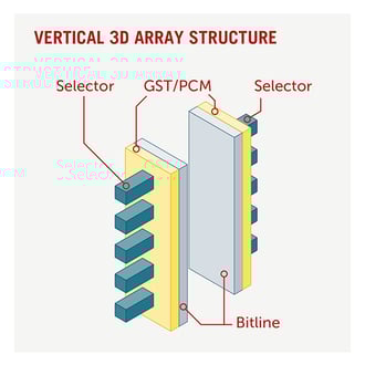
Such a structure was proposed as early as 2012, but commercial production remains elusive. Producing it with a high enough yield is a big challenge. The answer lies in creative thinking. We can borrow and combine several approaches.
The overall structure for a vertical PCM configuration is made in a similar fashion to today’s 3D NAND devices. It requires depositing a conformal, smooth, and dense PCM film on the vertical sidewalls. Metal organic chemical vapor deposition (MOCVD) can achieve the necessary high-quality conformal film, but only if the deposition temperature is below the crystallization temperature of the PCM materials, which is typically ~200°C (~392°F).
Benchmark testing shows excellent performance on test PCM devices. More work is needed before the concept is ready for high-volume production. Still, all results indicate that PCMs deposited by MOCVD are suitable for high-performance SCM applications using creative 3D architectures.
If you are hunting for a better solution for your high-density, nonvolatile memory,
we can help you find the best combination of materials and structures to meet your needs.
Learn more about storage class memory!

