hero-654791312-sized

Ensights

Science that is transforming lives and enabling the future

Entegris and HOF begin Partnership to bring Added Value to Biopharm Bulk Drug Substance, Cold Storage, and Transport

All Posts

Entegris and HOF begin Partnership to bring Added Value to Biopharm Bulk Drug Substance, Cold Storage, and Transport

Entegris is proud to announce a new relationship with HOF Sonderanlagenbau GmbH, an international provider of freeze/thaw equipment and special solutions for the pharmaceutical and biotechnology sectors. Entegris offers the best-in-class Aramus™ bag for robust cold storage and transport. 

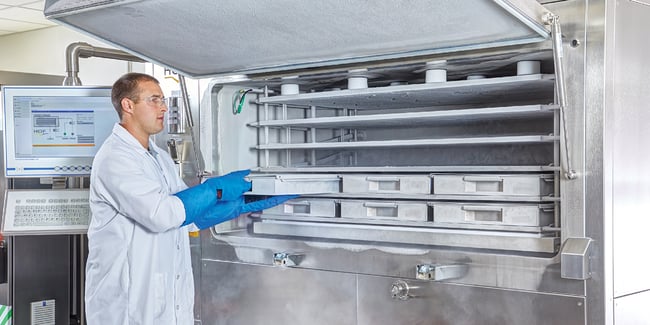
Collaborating with HOF enables Entegris to offer a combined solution for our customers that accelerate the freeze/thaw process and help showcase our new Life Sciences Technology Center, built to offer customers the opportunity to leverage our cold-chain supply expertise to optimize processes, reduce costs, and increase speed to market.


Having the HOF freeze/thaw unit placed within the Life Science Technology Center enables our customers the possibility of finding the best available solution for their individual process. This partnership increases our leading position in the market and facilitates US-based customers getting in touch with our equipment and identifying their unique single-use solution.

Our new Life Sciences Technology Center, located in Billerica, MA, will feature HOF freezers and offers life sciences customers the opportunity to leverage our expertise on cold-chain supply challenges to optimize processes, reduce costs, and increase speed-to-market. The world-class laboratory brings our tools and technologies together in one place, where customers can test equipment for freeze/thaw processes to determine which products best fit their needs.

We have developed a broad component ecosystem that can be configured to manage the most demanding process needs, and we’re excited to maximize the freeze/thaw benefits for the customer in our new partnership with HOF Freezers.
hof-collaboration-blog-inline-12549-1200x600

We invite you to our Life Sciences Technology Center Open House during BioProcess International, September 27-30.

Explore our cold-chain equipment, talk to our freeze/thaw experts, and learn how we can help you make the right choices to achieve your goals.

Related Posts

Exploring the Superiority of Silicon Carbide in Optical Components

Exploring the Superiority of Silicon Carbide in Optical Components Silicon carbide (SiC) is a leading material for high-performance optical components, offering numerous advantages over traditional materials such as glass and metal. Its exceptional specific stiffness, high thermal conductivity, and outstanding dimensional stability position SiC as a superior choice compared to beryllium and low-expansion glass ceramics. Historically, the high costs associated with the preliminary shaping and final finishing of SiC have hindered its widespread adoption in optical systems. The material is both hard and strong, requiring precision machining with expensive diamond tooling on high-quality, rigid machine tools. However, advances in manufacturing techniques, such as near-net-shape slip casting, have demonstrated success in reducing costs despite necessitating significant diamond grinding. Building on this success, Entegris offers an entirely new way of creating SiC. Using our chemical vapor conversion process, we can create net- or near net-shaped SiC components in complex forms while spending much less time on fabrication.

Designing for Extended Performance in Life Science Contaminant Removal

Designing for Extended Performance in Life Science Contaminant Removal Filters have a finite lifetime, and their performance also changes over time. How do you get the most performance over the longest lifespan?

Entegris Offers New FOUP Form-Factors for Non-Standard Wafers

Entegris Offers New FOUP Form-Factors for Non-Standard Wafers Over the last few years, 3D stacking has gone from a relatively niche fabrication method to an absolute necessity for cutting-edge applications. As chipmakers delve into smaller and smaller nodes, stacking and die-bonding wafers has become a preferred way of creating more processing power in a smaller space. Stacked and bonded wafers don’t behave the same way as 2D wafers: Wafers are thinned prior to bonding, which results in wafers that can sag when handled Bonded wafers are thicker and heavier than 2D wafers when assembled Bonded wafers can also warp following assembly Many automation tools rely on the predictable geometry and characteristics of 2D silicon wafers for safe handling and transport. While stacked and bonded wafers are a game-changer for miniaturization, they can also force manufacturing compromises unless chipmakers adopt specialized tools for the back end of the line (BEOL).