Entegris recently participated at SEMICON West in San Francisco, CA, July 12 – 14. After three years without a major onsite presence, the team was eager to be back in person and engage face-to-face with key customers and suppliers.
This also marked the first major industry event with CMC Materials being part of Entegris. Following the close of the acquisition July 6, Entegris now offers the industry’s most comprehensive and innovative end-to-end electronic materials offering.
“The addition of CMC Materials’ suite of solutions allows Entegris to offer the industry’s most comprehensive portfolio and enhanced operating capabilities for applications in the fab environment and across the semiconductor ecosystem. SEMICON West provided the perfect opportunity for us to meet with investors, customers, and suppliers to share our excitement and the value this will bring to the industry,” said Bertrand Loy, Entegris president and CEO.
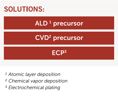
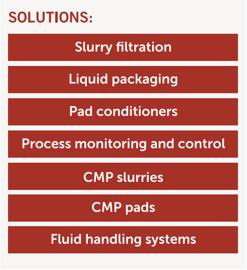
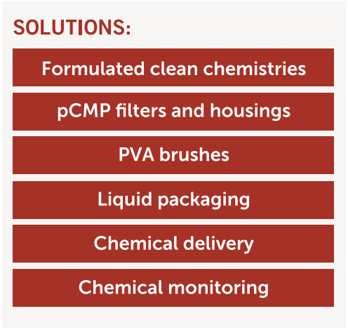
Integrated CMP Solutions
Faster time to co-optimized solutions and defect reduction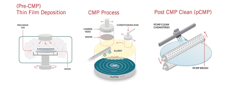
 |
 |
 |
On the first day of SEMICON West, Lam Research announced a strategic collaboration with Entegris and Gelest, Inc. in a news release. We invite you to read the news release and learn more about EUV dry resist precursors on our new resource page.
 Dry Resist process flow: Precursor canister delivery, dry deposition, EUV exposure, and dry develop.
Following the event, we caught up with Dr. David Medeiros, senior director of engineering for Entegris to learn about his experiences. Here is what he had to say:
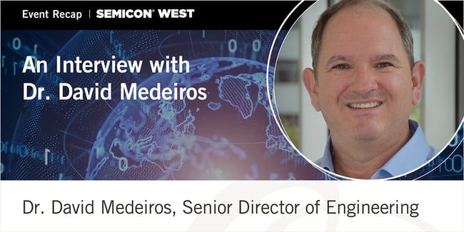
This is the first year back in-person at SEMICON West in quite some time. How was the overall attendance and what value did you find from being back onsite?
The presentations I attended were largely near capacity and the expo floor was also quite full. The biggest value being onsite is having face-to-face contact with colleagues and customers. The relationships established over the years are incredibly important, and with the isolation these past few years communication that best comes from in-person contact has been hindered. Plus, there are new connections established that would not occur without being physically present.
This was also the first year that SEMI introduced the Sustainability Summit. Can you share the major takeaways from this event?
SEMI brought together thought leaders across the industry to share perspectives on what sustainability means to them and their companies. Great presentations from semiconductor manufacturers and suppliers were complemented by a panel discussion on the industry’s focus on decarbonization.
There were interesting talks from outside of the semiconductor industry with compelling messages and great examples of using innovation to drive a value-add focus on sustainability efforts.
A near universal consensus was that sustainability efforts need to be highly collaborative across the industry. There was a strong push for interaction and engagement between suppliers, semiconductors manufacturers, and device designers, such as fabless companies. There was also a significant focus on the need to address all aspects of carbon emissions. While Scope 3 emissions generated from the end use of semiconductors are the largest contributor, Scope 1 and 2, from direct use in manufacturing or indirect from energy purchased or used in manufacturing, respectively, are more under direct control of companies like Entegris that are providing materials and products used in semiconductor production. Several discussions focused on the need to enable lower power consuming semiconductors to specifically address Scope 3 emissions.
How do these initiatives line-up with Entegris’ sustainability efforts?
It was encouraging to hear how the initiatives being highlighted by the industry leaders are so well aligned with Entegris’ sustainability program. Several companies reported 2030 goals similar to our objectives of reducing energy and water consumption and moving to renewable energy sources.
The work happening at Entegris’ Billerica and Yonezawa facilities on water conservation and the entire strategy for enabling the new Kaohsiung Science Park (KSP) facility in Taiwan with the goal of recycling 85% of its water used in operations and increasing the sourcing of renewable of energy are well aligned with the direction the industry is moving.
The move toward a more circular economy, meaning reducing the amount of waste generated in manufacturing through increased recycling, reuse, or reduction on consumables was also highlighted. This is well aligned with a new initiative we are establishing called Plastics Footprint Reduction, where we are developing programs that reduce the volume of plastic products we produce that may end up in landfills.
Kaohsiung Science Park (KSP) facility in Taiwan
Outside of sustainability, can you share any major industry trends that were discussed?
I listened to discussions on macroeconomic issues facing the industry and the potential for a recession. While there is a general view of the analysts that a recession is possible or even likely, there was also consensus that this was a ‘correction’ from the over-heated economy, and it would not impact the overall positive trajectory of growth in the semiconductor market.
Logic was viewed as moving favorably, while prices for memory may lag. There was a generally optimistic view for the long haul, with ‘bumps’ along the way, including the potential for slight overcapacity situation, which would eventually dissipate as demand continues. Considering the long lead time for capacity to come on board, in general, investments need to continue to meet an industry that maintains its path toward $1T around the end of the decade, plus or minus a few years. Of course, we would still see supply chain issues challenging the industry on many fronts as one speaker indicated that it has been reported that there are 62 fabs being constructed or planned to start construction in the next two years, worldwide! This would be a mix of 300mm, 200mm and smaller wafer size fabs, but the magnitude of investment suggests that growth in demand is projected to continue for several years.
There was also a great discussion about the CHIPS (Creating Helpful Incentives to Produce Semiconductors) for America Act, which is currently being negotiated in Congress. The Act, if passed, would allocate $52B over five years to provide incentives for new manufacturing in the USA as well as a significant fund to enable a National Semiconductor Technology Center (NSTC) to promote renewed focus on manufacturing excellence, domestic supply chain and workforce development.
Is there anything else you’d like to share from your experience at SEMICON West?
I thought the conference was a success! The presentations confirmed many of the projects we are working on at Entegris are well positioned for the needs of the industry in terms of increased capacity, technological advances, and focus on sustainability. The face-to-face interactions with colleagues from across the semiconductor industry and around the world, provided invaluable input to help develop and refine our strategies as a technology leader in yield-enabling materials and solutions
Forward Looking Statements
This communication contains forward-looking statements. The words “believe,” “expect,” “anticipate,” “intend,” “estimate,” “forecast,” “project,” “should,” “may,” “will,” “would” or the negative thereof and similar expressions are intended to identify such forward-looking statements. These forward-looking statements include statements related to Entegris’ acquisition of CMC Materials, Inc.; the strategic collaboration among Entegris, Lam Research and Gelest, Inc.; Entegris’ corporate social responsibility program, including goals related to sustainability; macroeconomic, industry and market trends; potential impacts of the CHIPS Act; and other matters. These statements involve risks and uncertainties, and actual results may differ materially from those projected in the forward-looking statements. These risks and uncertainties include, but are not limited to, those risk factors and additional information described in Entegris’ filings with the Securities and Exchange Commission, including under the heading “Risk Factors” in Item 1A of Entegris’ Annual Report on Form 10-K for the fiscal year ended December 31, 2021, filed with the Securities and Exchange Commission on February 4, 2022, and in Entegris’ other periodic filings.


