 What do plasma chamber components have to do with deer or wild boar? These animals are potential sources of food for the tiger. The components are potential sources of contamination in the fab. Success in both cases relies on attention to detail and a flexible strategy. Whether you are chasing prey or particle contamination, a multi-pronged approach is best.
The goal of the wafer fab operator is to control contaminants and improve yield.
At the 10-nanometer scale and below, every process tool or piece of equipment can be a potential source of contamination. Semiconductor manufacturers are on the prowl, seeking out techniques that will allow them to stop contamination at the source. One such source that is sometimes overlooked is the components inside a deposition chamber. Danger lurks around every crevice.
Coating Chamber Components
Components are often made from anodized aluminum or other metals coated with oxides. Plasma spray coating of yttrium oxide has long been the industry norm. These conventional oxide coatings protect components inside the chamber and in the gas and chemical delivery systems. The coatings extend the life of the parts but may not provide the necessary contamination control and chemical stability for processing at advanced nodes with complex architectures.
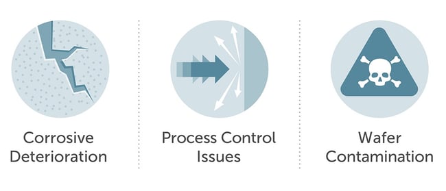
Problems arise when the coatings used to protect components from damage during etching and deposition processes wear off. Worn coatings shed particles that make consistent process control more difficult and can cause yield loss. Conventionally coated components are not rugged enough to withstand the demands of longer etching times and hotter plasma temperatures.
Suppliers need to seek different methods of protecting components. Coatings must:
- Adhere strongly to the substrate
- Resist chemical attack and oxidation
- Withstand wear and corrosion
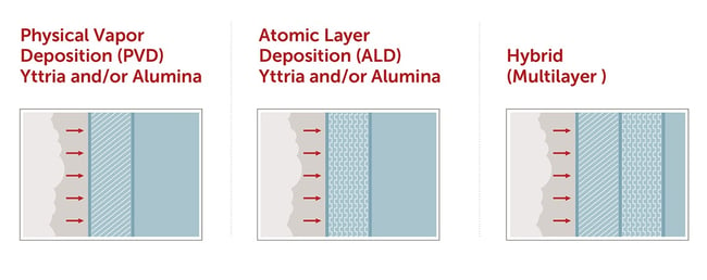
 Thin film technologies developed for wafer processing offer a solution. There are two options: physical vapor deposition (PVD) or atomic layer deposition (ALD).

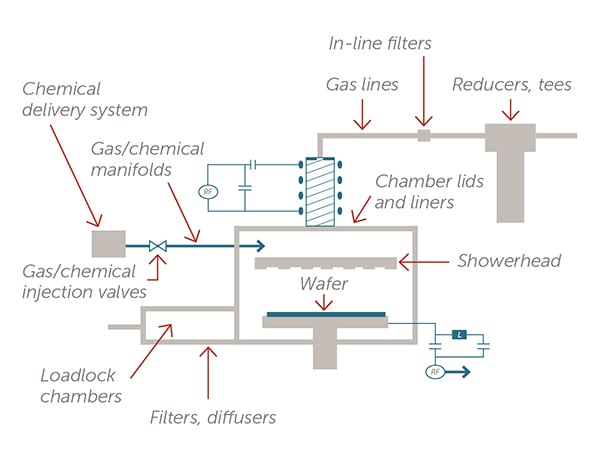
Figure A: Components in a typical deposition chamber that can be coated by PVD and/or ALD coatings.
Parts shaded in gray are examples of various components in a typical deposition or etch chamber.
Which strategy is best? The optimal coating approach depends on the chamber type, the geometry and material of the component, and processing conditions. There are always trade-offs.
Advantages of PVD
The PVD coating method is relatively fast, which makes it best suited in applications where thicker coatings are needed to adequately resist damage from the corrosive etchants. This is the case in etching tools, where parts are exposed to plasma for a long time. For example, channels in 3D NAND devices can be 5 µm thick and must
be etched from top to bottom. PVD-coated components can withstand the long etching times without degrading.
PVD yttria and alumina produce much denser and cleaner coatings than the standard plasma spray methods, reducing the risk of particle generation resulting from coating degradation. The agglomeration that occurs during plasma spraying is not an issue for PVD coatings. PVD creates uniform, dense coatings that protect the parts. The PVD method is flexible. Many possible source materials are available for the targets, and it is relatively easy to adjust the process accordingly.
Advantages of ALD
ALD is an excellent method to produce dense, pinhole-free coatings on any component. It can fill narrow, deep holes and produce highly conformal coatings
that encapsulate a part. The process applies to both etching and deposition tools.
Intricate chamber components especially benefit from the precision of ALD. Showerheads, for example, often contain thousands of tiny holes and sometimes have internal channels that cannot be adequately coated with any other method. Because they deliver chemicals directly to the wafer surface, particle control is especially critical.
A Multi-Pronged Approach
Equipment suppliers do not need to limit their options to coating components with
a single material or solely with either PVD or ALD. Sometimes a hybrid or composite approach makes the most sense.

Each technique has limitations. PVD requires a line of sight, making it difficult to adequately coat some component geometries. ALD can coat parts of any shape,
but it is a slow process and, therefore, more expensive than PVD.
Line of sight and speed are also essential considerations for tigers when choosing which prey to target. They rely on sight to spot prey and can only sprint for a short distance, so they need to be flexible and go after whatever game is most likely to yield them a catch. Are deer or wild boar more plentiful? Surroundings matter, both in the savanna and in the fab. Choose the coating technique wisely, and your plasma chamber components will last longer while allowing you to maintain a high yield.
To learn more, visit our Advanced Deposition Solutions page.


