


Hydrogen composes about 75% by mass of the normal matter in the universe, existing as H2 gas under s...

Science that is transforming lives and enabling the future
Hydrogen composes about 75% by mass of the normal matter in the universe, existing as H2 gas under standard conditions. This abundance of supply creates opportunities in numerous applications, including semiconductor manufacturing, for which hydrogen is considered a bulk gas and is employed in many parts of the ecosystem.
Last year, Semiconductor Digest assembled six panelists from the world's leading semiconductor and automotive manufacturers and suppliers - including Volkswagen, Texas Instruments, Robert Bosch, Hyperion, and KLA, and Entegris - and asked them about the state of automotive electronics. They discussed issues such as the shift to automotive quad computing, the emphasis on infotainment, and the rise of alternative vehicle technologies such as electrification and self-driving.
Growth is good; no one in the semiconductor industry would argue this point. And according to Gartner, there’s a lot of “good” on the horizon. Current forecasts call for semiconductor sales to more than double in this decade, going from $400 billion in 2020 to $1T by 2030. With growth, however, come growing pains. To reach the heights of $1T-plus in semiconductor sales, the industry must evolve by significantly increasing not only the amount of wafers and wafer starts annually but also the amount of investment in equipment and materials. Semiconductor materials consumption during the same decade is expected to double as well. This creates great opportunity for materials suppliers, but it also will mean taking a hard look at the materials supply chain – what are the challenges, and how can they be addressed?
Changing one material in the semiconductor manufacturing process has a cascading effect on multiple process steps. Consider the replacement of tungsten (W) and copper (Cu) with molybdenum (Mo). Integrated device manufacturers (IDMs) are implementing Mo in advanced designs, focusing on 2-nanometer (nm) nodes and below. Mo is highly conductive, can be deposited without a titanium or titanium nitrid
Silicon carbide (SiC) has become popular with chipmakers. Its wide-bandgap structure offers many design benefits for the operations of power semiconductors. Compared to silicon, SiC wafers enable the fabrication of faster, more efficient devices that can both operate at higher temperatures and remain stable when deployed in extreme temperature environments. Processing SiC wafers using the same materials and methods as silicon wafers is not a viable option, however.
If you asked a semiconductor process engineer to name their biggest challenge when tackling the next technology node, they would likely tell you it is figuring out how to achieve high device yields. This is mainly due to an increase in possible points of contamination as the number of potential contaminants grows and their sizes shrink. It is becoming particularly difficult to detect metal contaminants and pinpoint their root cause so they can be eliminated. That’s because they can form anywhere in the process flow.
In the early days of semiconductor manufacturing, fabs would remove contaminants from their process fluids in a sequence that could be analogized to making a cup of coffee. By using a filter with tiny pores, large contaminants (coffee grounds) are separated from water. Because the coffee grounds are too large to pass through the filter, they can’t pass into the coffee we drink.
For decades, the semiconductor device manufacturing mantra was “How do we make them smaller, cheaper, and faster?” The pursuit of Moore’s Law – the doubling of transistors on a chip every two years – was achieved through planar scaling. But that approach could only go on for so long. The mantra now is “How do we improve power, performance, area, and cost (PPAC)?” At the 14 nm node, it was clear that the best way to push the limits of semiconductor device PPAC was to take it into the third dimension.
Things are not always as they appear. Take semiconductor manufacturing. On the surface, it may seem that the secret to making semiconductor devices more advanced lies in the design. But just as an architect’s design for a building may not be structurally feasible without the right materials, a semiconductor device design may not be functional if the materials and their interactions are not considered and optimized.
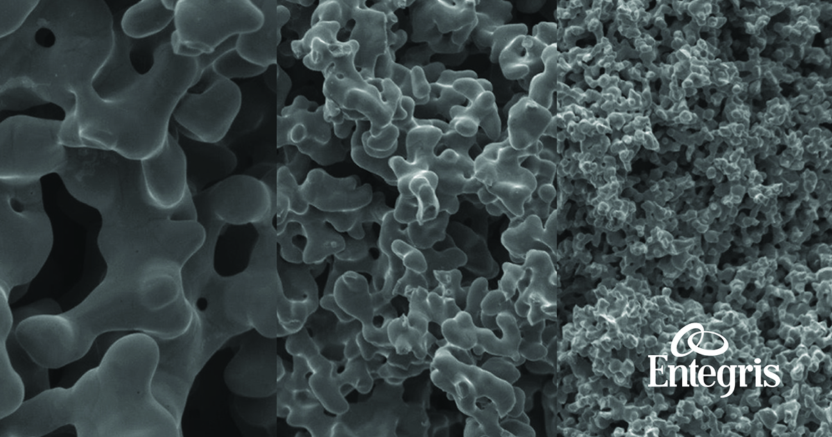
Here’s a challenge, say the number 9 out loud, nine times. 9, 9, 9, 9, 9, 9, 9, 9, 9.
Whether it is a deliberate strategy or serendipity, the innovations that shape our lives are the result of skilled people put into the right environment to create something new. Innovation is not an exact science, but persistence and some good luck have yielded all the amazing tools and technology we rely upon.
Entegris recently participated at SEMICON West in San Francisco, CA, July 12 – 14. After three years without a major onsite presence, the team was eager to be back in person and engage face-to-face with key customers and suppliers.
Hydrogen composes about 75% by mass of the normal matter in the universe, existing as H2 gas under s...

Last year, Semiconductor Digest assembled six panelists from the world's leading semiconductor and a...
Growth is good; no one in the semiconductor industry would argue this point. And according to Gartne...

Changing one material in the semiconductor manufacturing process has a cascading effect on multiple ...

Silicon carbide (SiC) has become popular with chipmakers. Its wide-bandgap structure offers many des...

If you asked a semiconductor process engineer to name their biggest challenge when tackling the next...

In the early days of semiconductor manufacturing, fabs would remove contaminants from their process ...

For decades, the semiconductor device manufacturing mantra was “How do we make them smaller, cheaper...

Things are not always as they appear. Take semiconductor manufacturing. On the surface, it may seem ...
Here’s a challenge, say the number 9 out loud, nine times. 9, 9, 9, 9, 9, 9, 9, 9, 9.

Whether it is a deliberate strategy or serendipity, the innovations that shape our lives are the res...

Entegris recently participated at SEMICON West in San Francisco, CA, July 12 – 14. After three years...
© 2026 Entegris. All Rights Reserved


