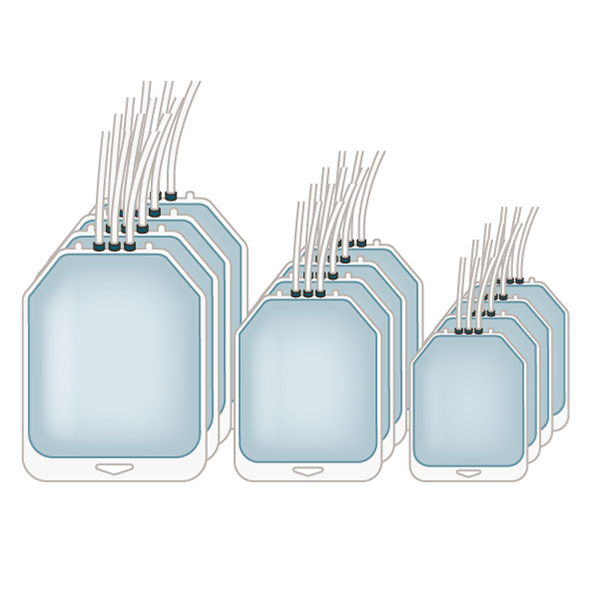
Why Switch to our Bags? Supply chain issues? Breaking bags? Freezing problems? Our Aramus™ bags can ...

Science that is transforming lives and enabling the future
Why Switch to our Bags? Supply chain issues? Breaking bags? Freezing problems? Our Aramus™ bags can get you back to making lifesaving therapeutics.
Freezing down bulk drug substance (BDS) isn’t something you can play around with. This is a high value product where any failure or contamination due to the bag breaking can lead to delays in medicine getting to the patient. Making sure you pick the right solution to protecting that product makes a big difference. Here are three questions you should be considering:
Since the introduction of the mobile phone, scientists and engineers have been on a series of quests to make them smaller and smarter. And incarnation after incarnation, from shoe box large to smart phone tiny, they succeeded. Until, that is, demand for more data, more storage, faster speeds, and longer battery life created major roadblocks. New smartphone capabilities — from biometrics to more accurate geopositioning, from artificial intelligence to virtual reality — demanded significant improvements in chip power. Their constant use required pronounced leaps in battery life.
The impact of the freeze/thaw process on workflows requires it be treated as a unit operation of its own.
As a partner, Entegris is continuously developing solutions for our customers’ biggest challenges. An unprecedented pandemic came with a one-of-a-kind challenge: help a leading COVID-19 vaccine manufacturer scale up their process.
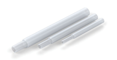
The pharmaceutical and biopharmaceutical industries continue to embrace the utilization of single-use systems (SUS). With the ever-growing adoption of SUS products, increasing scrutiny has been placed on the purity concerns of single-use components and their possible impact on the biomanufacturing, storage and transportation of high value final products.
Advanced 3D architectures for logic and memory devices increasingly rely on atomic layer deposition (ALD) to achieve high-quality, nanoscale conformal coatings. ALD deposits reactants and precursor molecules in alternating pulses to create the desired chemical makeup of the layers. Because of its ability to produce extremely thin films of uniform thickness and composition, ALD has supplanted physical vapor deposition (PVD) as the dominant deposition process for leading-edge technology nodes.
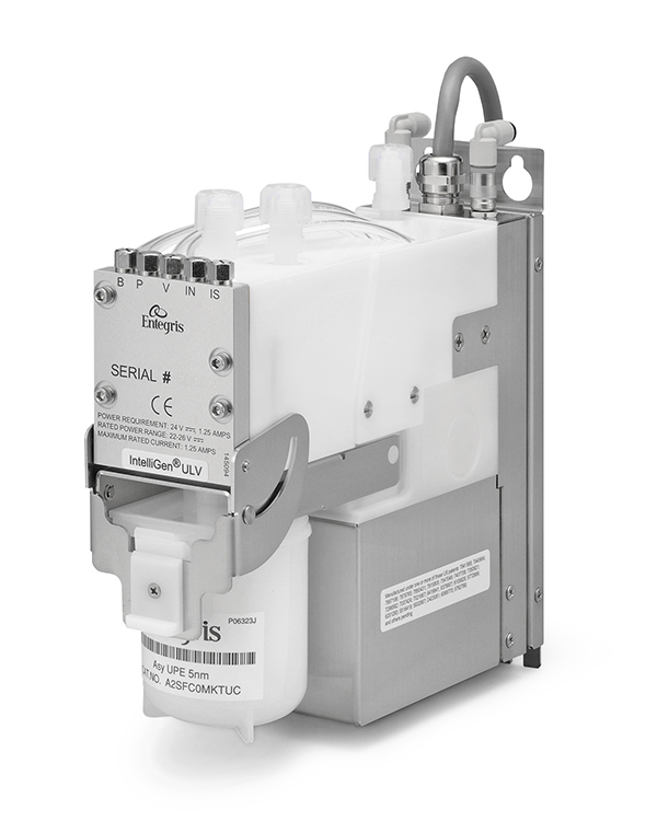
The purpose of a CMP process is simple – to planarize the top layer of oxide or metal with an abrasive slurry. Manufacturing the slurry to the exacting standards required by the end user is not easy. To effectively planarize the wafer surfaces, both large and small abrasive particles must be removed prior to being dispensed. Thus, the target is a narrow particle size distribution between 30 and 200 nm to prevent both microscratches and underlayer defects.
Simplify your operations and supply chain with a versatile contamination control strategy.
Overview The rapid increase of semiconductors in cars enables significant safety, connectivity, mobility, and sustainability improvements. As transportation transforms from being driver controlled to software controlled, automakers must look closer at their ability to measure and maintain product reliability throughout the vehicle’s lifetime.
Electronic devices now serve as the backbone of modern vehicles and have become the focus of quality standards that ensure automotive functional safety. As automakers transform their organizations to adapt and become experts in manufacturing digital machines, current gaps in how the automotive and semiconductor supply chains interact have emerged.
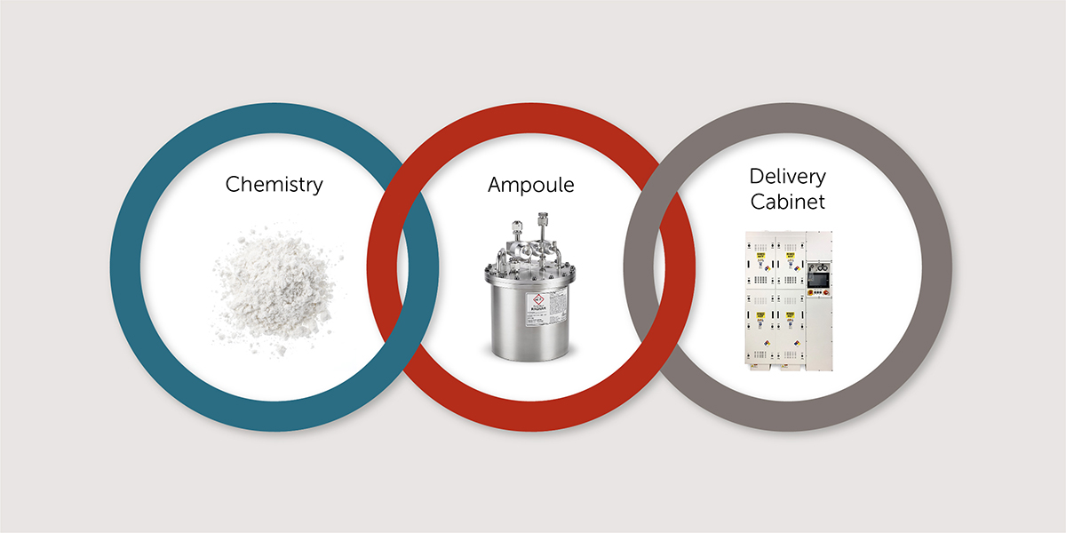
A high purity sub-fab serves as the central nervous system of a semiconductor cleanroom. It houses chemical delivery, purification, recycling, and destruction systems. The sub-fab is where potentially hazardous aqueous chemistries and gases are stored and handled until they are delivered to the cleanroom process equipment located either in the floor above it or the building adjacent to it.
Why Switch to our Bags? Supply chain issues? Breaking bags? Freezing problems? Our Aramus™ bags can ...

Freezing down bulk drug substance (BDS) isn’t something you can play around with. This is a high val...

Since the introduction of the mobile phone, scientists and engineers have been on a series of quests...

The impact of the freeze/thaw process on workflows requires it be treated as a unit operation of its...

As a partner, Entegris is continuously developing solutions for our customers’ biggest challenges. A...

The pharmaceutical and biopharmaceutical industries continue to embrace the utilization of single-us...
Advanced 3D architectures for logic and memory devices increasingly rely on atomic layer deposition ...
The purpose of a CMP process is simple – to planarize the top layer of oxide or metal with an abrasi...

Simplify your operations and supply chain with a versatile contamination control strategy.
Overview The rapid increase of semiconductors in cars enables significant safety, connectivity, mobi...

Electronic devices now serve as the backbone of modern vehicles and have become the focus of quality...
A high purity sub-fab serves as the central nervous system of a semiconductor cleanroom. It houses c...
© 2026 Entegris. All Rights Reserved

