Overview The rapid increase of semiconductors in cars enables significant safety, connectivity, mobi...

Science that is transforming lives and enabling the future
Overview The rapid increase of semiconductors in cars enables significant safety, connectivity, mobility, and sustainability improvements. As transportation transforms from being driver controlled to software controlled, automakers must look closer at their ability to measure and maintain product reliability throughout the vehicle’s lifetime.
A high purity sub-fab serves as the central nervous system of a semiconductor cleanroom. It houses chemical delivery, purification, recycling, and destruction systems. The sub-fab is where potentially hazardous aqueous chemistries and gases are stored and handled until they are delivered to the cleanroom process equipment located either in the floor above it or the building adjacent to it.
The electric vehicle (EV) market is expanding in response to customer demand, with multiple major automotive companies offering lower cost models with longer driving range.
Migration from 2D to 3D structures for high-density memory devices changes the nature of etching and deposition processes, especially as the number of layers for 3D NAND integration grows to 96 and beyond, and new process chemistries become commonplace. The greater number of lengthy processing steps and high aspect ratio (HAR) features involved place new demands on all steps of the chip manufacturing process, including etching, deposition, and cleaning equipment. Consistent process stability becomes harder to achieve.
Much as a bolt of lightning can strike in one spot and travel, creating a path of destruction in its wake, a single electrostatic discharge can have a similar effect on a semiconductor manufacturer’s bottom line. For advanced-node manufacturers, the risk posed by electrostatic discharge has become amplified by the move to fluoropolymers, a consequence of stainless-steel process tool components failing to meet increased purity requirements.
Entegris recently wrapped up an exciting week at the first-ever SEMICON West virtual event. The event provided a great opportunity to connect with the community and gain valuable insight into the future of the industry.
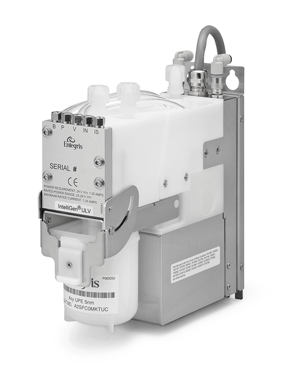
Photochemicals are playing an increasingly important role in bringing next generation devices to reality. While semiconductor manufacturing has always needed a pure, contamination-free environment, the requirements are tightening even further.
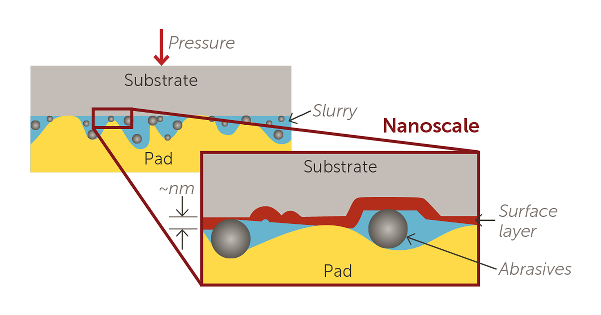
To meet increasing sensitivity to contaminants in integrated circuit (IC) manufacturing, semiconductor fabs have begun looking to their chemical suppliers to adopt new contamination control standards that improve quality and assist in reducing wafer defects. Each material has several touch points along the chemical manufacturing, storage, transport, and delivery journey that could add or generate contaminants. Semiconductor fabs seek assurance from their materials suppliers that they will minimize opportunities for contaminants to end up on a wafer (Figure 1).
Ensuring Purity and Safety Purity requirements continue to tighten as the semiconductor manufacturers continue to pursue advanced technology nodes. Of all the industries that rely on a consistent supply of both raw and specialty chemical, the semiconductor industry sets the highest bar.
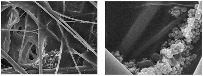
Dewetting and non-dewetting are not common terms used every day, yet are vital to the functionality of liquid filters.
Wetting the membrane is an important first step in preparing your filter. Wetting the membrane pores eliminates dry pathways where contaminants, like particles, gels, or bubbles could pass through, resulting in high defect levels in your process. Polymer membranes are natively hydrophobic or hydrophilic.
Overview The rapid increase of semiconductors in cars enables significant safety, connectivity, mobi...

A high purity sub-fab serves as the central nervous system of a semiconductor cleanroom. It houses c...
The electric vehicle (EV) market is expanding in response to customer demand, with multiple major au...
Migration from 2D to 3D structures for high-density memory devices changes the nature of etching and...

Much as a bolt of lightning can strike in one spot and travel, creating a path of destruction in its...

Entegris recently wrapped up an exciting week at the first-ever SEMICON West virtual event. The even...

Photochemicals are playing an increasingly important role in bringing next generation devices to rea...
To meet increasing sensitivity to contaminants in integrated circuit (IC) manufacturing, semiconduct...

Ensuring Purity and Safety Purity requirements continue to tighten as the semiconductor manufacturer...

Dewetting and non-dewetting are not common terms used every day, yet are vital to the functionality ...

Wetting the membrane is an important first step in preparing your filter. Wetting the membrane pores...
© 2026 Entegris. All Rights Reserved

