Much as a bolt of lightning can strike in one spot and travel, creating a path of destruction in its wake, a single electrostatic discharge can have a similar effect on a semiconductor manufacturer’s bottom line. For advanced-node manufacturers, the risk posed by electrostatic discharge has become amplified by the move to fluoropolymers, a consequence of stainless-steel process tool components failing to meet increased purity requirements.
THE TRANSITION FROM STAINLESS STEEL TO PFA TUBING
Emerging technology breakthroughs like artificial intelligence (AI), 5G, and the internet of things (IoT) are driving the semiconductor industry to advanced technology nodes and heterogeneous integration. At the same time, these applications are driving a need for higher reliability devices; as the need for autonomous vehicles and medical devices increases, device failure is not an option.
To achieve the performance needed for these advanced technologies, chips must be designed with ever-smaller feature sizes and higher-density interconnects. Some of the most consequential impacts of meeting these design requirements are that photolithography and wet etch and clean processes have become more metal sensitive at advanced nodes. Because the process chemicals used can extract metals from the stainless-steel components and lead to wafer defects and yield loss, most stainless-steel fluid handling systems are no longer able to meet purity specifications.
The increasing requirements for material and chemical purity have led many manufacturers to convert their stainless-steel fluid handling systems to perfluo-roalkoxy (PFA), a common fluoropolymer. While this successfully reduced the presence of extracted metals, the increased use of fluoropolymer systems creates new concerns associated with electrostatic charge generation, accumulation, and harmful discharges in components such as PFA tubing, fittings, and other components.
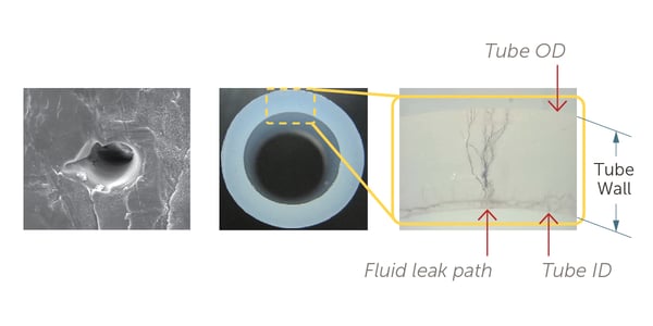
- Safety Risks – solvents used in semiconductor manufacturing processes have low conductivity, which enables them to generate and accumulate an electrical charge. Propagating electrostatic discharges can be powerful enough to cause “pinhole” damage to the components, causing leaks that contaminate the process. Furthermore, electrostatic discharges generated in fluoropolymer systems that are transferring flammable solvents can create leak paths through the tubing that could possibly ignite the surrounding, potentially flammable solvent-rich environment, Figure 1.
- Impact on Cost of Ownership – beyond safety hazards, harm caused by electrostatic discharges can have a significant impact on cost of ownership because it can shorten the life of critical process tools and components in a semiconductor fab.
-
Impact on Device Yield – the presence of large electrical potential in process chemistries can not only damage the tubing and components in the flow path, it can also directly damage semiconductor devices on the wafers themselves.
 |
THE RIGHT SOLUTION
Several attempts have been made to mitigate electrostatic hazards in PFA tubing such as replacing it with tubing that uses a conductive carbon stripe on the outside of the tube only, or utilizing tubing with a continuous conductive element from the interior of the tubing to the exterior. There have even been attempts to alter the chemistry itself. Each of these methods has fallen short by addressing some of the electrostatic hazard challenges but not preventing on-wafer damage caused by electrostatic charge accumulation on the flowing liquid itself, or by adding complex wiring to bring separate tube sections to ground and creating potential strength and safety concerns of the overall system, or by adding unacceptable cost and downtime.
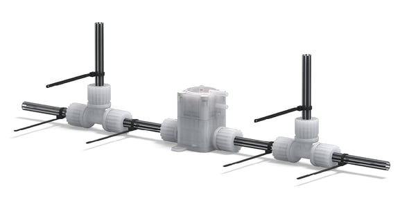
Innovating even further led Entegris to successfully develop a continuously conductive PFA fluid handling system that removes the charge from the media, reduces required ground wiring, maintains tubing strength, and allows an uninterrupted dissipation path to ground throughout the entire fluid circuit, Figure 2.

|
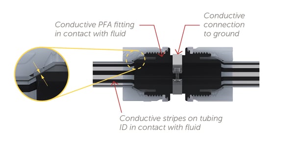
Designed from a new material, the tubing has carbon stripes along the inside and the fittings are carbon-loaded to create a path to ground when the sealing area contacts the conductive stripe, Figure 3.
 |
This system has proven to successfully reduce the accumulated electrostatic charge from both the media flowing through the tubing as well as any charge that might build up inside the tube, mitigating safety and financial risks.
To learn more about properly managing ESD in your manufacturing environment and discover our innovative solutions that address the semiconductor industry’s need to remove charge from process chemicals and control contamination, visit www.entegris.com/esd.


