

The electric vehicle (EV) market is expanding in response to customer demand, with multiple major automotive companies offering lower cost models with longer driving range.
Automotive components continue to improve to meet this need. Batteries are operating at higher voltage and circuits are operating at higher frequency. As battery voltage increases to 650V, 1200V, or even higher, power integrated circuit (IC) manufacturers must produce chips that can withstand high-temperature, high-frequency operating environments.
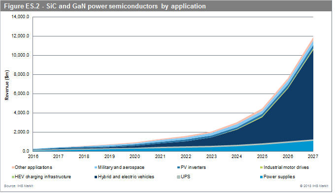
The automotive industry is currently facing a supply shortage for many of the chips required to produce today’s vehicles, let alone the volumes that will be required in coming years to meet the expected market growth, Figure 1. This includes power ICs for EVs.
 |
High-performance power ICs are often based on silicon carbide (SiC) substrates. SiC can tolerate much higher temperatures than silicon or gallium nitride (GaN) and improve device electrical performance. In terms of switching efficiency, SiC outperforms silicon by an order of magnitude.
The automotive market conditions provide both a challenge and an opportunity for the semiconductor industry.
The role of CMP
With the difficulty in ensuring an adequate supply of SiC wafers, solutions that improve throughput and reduce cost of ownership (COO) will be especially valuable. This is where chemical mechanical planarization (CMP) comes into play.
Manufacturing of SiC wafers from SiC boules begins with sawing, grinding, lapping, and polishing to create a smooth finish for subsequent epitaxial deposition. CMP processes that are optimized for SiC wafers support higher yield and lower scrap rates, thereby mitigating the supply chain challenges.
Wafer size is another factor to consider. As the SiC market moves from 150 mm to 200 mm wafers, manufacturers must contend with the greater challenge of achieving a planar, uniform surface across the entire wafer. Fabs are likely to transition from batch polishing tools to those that process one wafer at a time, putting pressure on throughput.
Lapping and polishing must be improved to take advantage of the process efficiencies that larger wafers enable. Higher polish rates are necessary, but faster polishing must not sacrifice surface quality.
SiC is a hard, chemically inert material that is much more difficult to polish than silicon. Standard CMP abrasives like silica and alumina result in extremely low material removal rates and, therefore, long polishing times.
Merely increasing the abrasive content to achieve faster material removal is not an optimal solution. Doing so will make the slurry more expensive while also increasing the incidence of scratches that cause defects. Similarly, increasing the pressure also induces undesirable scratches on the wafer.
Improving yield and throughput
Yield improvements depend on implementing advanced CMP processes but also in adjustments to the steps before polishing. Grinding and lapping the SiC wafer with diamond particles removes the marks from sawing but also introduces sub-surface damage. Standard micron-scale diamond slurries used for grinding achieve fast material removal rate, but at the expense of relatively rough surfaces.
For the lapping step, slurry formulations that incorporate smaller proprietary engineered nanodiamond particles can achieve rapid enough SiC removal with minimal sub-surface damage. By using engineered nanodiamond particles, the lapping process creates a smoother surface that will better prepare the wafer for CMP.
The challenge of efficient CMP on SiC wafers can now be solved by migrating away from conventional CMP slurry formulations to customized particles and additives selected to enhance the surface reaction kinetics of SiC. A method called reactive CMP uses precise, localized chemical reactions to achieve high removal rates along with improved surface finish.
Polishing pads must also be optimized so that CMP can be performed with lower pressure while polishing uniformly across the wafer. This is critical because flatness specifications are more stringent for 5G operations than they were for 4G. Also, fine scratches that were previously accepted now create reliability issues.
As performance demands are increasing, so are cost pressures. The tight SiC supply means that producing more good wafers per ingot is critical. The combination of lapping and polishing techniques described above addresses this need. The resulting improved finish of the base layer allows subsequent patterned layers to achieve lower defect rates and, therefore, higher device yields.
To learn more about advanced SiC CMP to support the expanding EV market as well as other applications for high-performance power ICs, see the Entegris white paper, “Advanced CMP of Silicon Carbide for EVs and Power ICs.”

