

Migration from 2D to 3D structures for high-density memory devices changes the nature of etching and deposition processes, especially as the number of layers for 3D NAND integration grows to 96 and beyond, and new process chemistries become commonplace. The greater number of lengthy processing steps and high aspect ratio (HAR) features involved place new demands on all steps of the chip manufacturing process, including etching, deposition, and cleaning equipment. Consistent process stability becomes harder to achieve.
The environment inside plasma etch and deposition chambers is just one example of an area that needs to be kept extremely clean and free of impurities, both to avoid yield loss and to maintain process stability for consistent results from wafer to wafer. Precise control of the process tool component surfaces in the etch chamber is necessary to maintain the desired etch rate and in deposition chambers to maintain the electrical integrity of deposited layers.
COATING CHAMBER PARTS AND COMPONENTS
Deposition chambers contain various parts and components that either contact the device wafer directly or are exposed to process chemicals that subsequently reach the wafer, Figure 1. As such, material selection is critical.
The corrosive chemicals used in plasma-etch chambers attack the tool component surfaces and degrade coatings. Longer exposure to hotter plasmas, which is common for 3D device processing, accelerates degradation. Particles shed from the corroded surfaces then deposit on the wafers, potentially causing device failure.
Components protected with yttrium oxide deposited by plasma spray-coating or made from anodized aluminum have long been the industry norm. Although such solutions have worked for many years, the nano-scale features of advanced process nodes demand an increased level of cleanliness for every part in the system. Conventionally coated components are not rugged enough to withstand the aggressive environments inside etch and deposition chambers without impacting device yield. Plasma spray coatings are relatively rough and porous, while anodized coatings exhibit in-situ cracking that makes them degrade too readily. The complex shapes of parts inside deposition chambers also pose a challenge for spray coating, which works best when coating planar surfaces.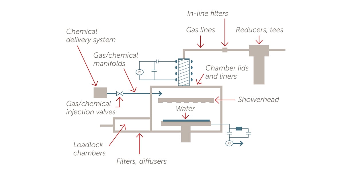
Figure 1. Components in a typical deposition chamber
that can be coated by PVD and/or ALD coatings.
PRECISION ENGINEERED COATING METHODS FOR HIGHER YIELD
Precision engineered, specialized coatings borrow vacuum thin film technologies associated with semiconductor wafer processing to produce coated components that can better resist the corrosion and oxidation that degrade conventional coatings. Two options are available: physical vapor deposition (PVD) and atomic layer deposition (ALD).
PVD and ALD coatings for chamber components are typically based on yttrium or aluminum oxides or may be made from aluminum oxynitride (AlON). The exact chemistry and coating thickness must be tailored to the application. The use of temperature in the chamber, processing time, and gases vary considerably depending on the device specifications, and these variables are used to select the right combination of coatings for their desired coating performance. Custom precision-engineered coatings provide the optimal balance between cost and performance.
Every precision engineered coating must exhibit a minimum level of wear and corrosion resistance in the presence of corrosive plasma/chemistry and adhere fully to the underlying substrate to create a uniformly coated surface. The geometry and material of the part being coated, the type of chamber, and the processing conditions further dictate the optimal coating chemistry and method.
PVD COATING METHOD
The PVD coating method is best suited for use in etching tools, where thicker coatings are needed to adequately resist damage from the corrosive etchants. The concern about coating integrity is especially critical when building challenging structures such as 3D NAND. The critical memory array channel and slot dry-etch steps are the most challenging, requiring high bias, long etch times to fully etch the 5-micron-thick structures from top to bottom. During this time, the etch chamber parts are exposed to aggressive, hot plasma.
PVD yttria or alumina produce much denser and cleaner coatings than standard plasma spray methods, reducing the risk of particle generation resulting from coating degradation. Since plasma spray coatings are formed by agglomeration of loosely generated particles with a porous microstructure, there is a tendency to etch around these agglomerations. The etched agglomerations rain down on the wafer as discrete particles. Because PVD coatings are dense they etch at a slower rate, coating the entire surface evenly, which maintains coating integrity.
PVD coating methods also allow for quick development of new coating materials by changing the source materials (targets). The process space can be quickly mapped for new materials using statistical techniques. Starting with an ultra-high-purity PVD target the film purity can be controlled. When using deposition tools with multiple sources, the coatings can be highly customized, creating complex alloys, oxides, and nitrides.
ALD COATING METHOD
ALD is ideal for coating components in both etch and deposition tools. Parts with complex interior geometry such as gas distribution components are especially suitable to an ALD coating process. Shower heads often contain thousands of small holes and sometimes even have internal channels or plenums, and because they deliver corrosive chemicals directly to the wafer surface, extreme cleanliness and corrosion resistance is critical.
ALD coatings will cover all surfaces and provide a reliable, high-purity, nearly defect-free protective barrier.
ALD is precise, but it is a relatively slow process. As such, it is best suited to applications where its unique attributes merit a higher up-front coating cost. For critical applications, the advantages of extended component life and reduced contamination provide an overall reduction in the cost of ownership.
MULTILAYER AND HYBRID APPROACHES FOR MAXIMUM FLEXIBILITY
Equipment suppliers do not need to limit their options to coating components with a single material or solely with either PVD or ALD. Sometimes a hybrid or composite approach makes the most sense.
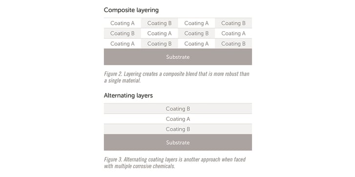
An ALD-only multilayering approach enables ultimate customization. Coating suppliers can deposit different materials for each ALD layer, creating a composite blend that is more robust than a single material for environments that face exposure to multiple corrosive chemicals, Figure 2 and Figure 3. A heterogeneous coating may withstand the varying chemical environment better than a homogeneous coating. Multilayering, may also combine layers deposited with ALD plus additional layers deposited with PVD, conveying the benefits of both processes.
 SUMMARY
Advanced semiconductor devices demand tools that facilitate high throughput and high yield while accommodating stringent contamination requirements and HAR geometries. Etch and deposition tools will only be able to meet these needs when chambers maintain an unprecedented level of cleanliness. Precision-engineered coatings on parts and components, deposited using PVD, ALD, or a combination of both techniques, address the limitations of conventional coating methods.
Regardless of the coating chemistry and deposition method, wafer manufacturers should expect PVD-and ALD-coated component suppliers to monitor the consistency of their coatings and provide guidance regarding coating selection. Optimal selection requires in-house testing in the exact manufacturing environment the components will experience. Tailoring a coating to an application should be a collaborative, iterative process that results in a precision-engineered coating. The benefits will be cleaner deposition chambers, reduced cost of ownership, and higher device yields.
To read the full paper, visit Entegris website: Advanced Coatings

