To meet increasing sensitivity to contaminants in integrated circuit (IC) manufacturing, semiconductor fabs have begun looking to their chemical suppliers
to adopt new contamination control standards that improve quality and assist in reducing wafer defects. Each material has several touch points along the chemical manufacturing, storage, transport, and delivery journey that could add or generate contaminants. Semiconductor fabs seek assurance from their materials suppliers that they will minimize opportunities for contaminants to end up on a wafer
(Figure 1).
 |
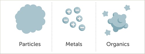
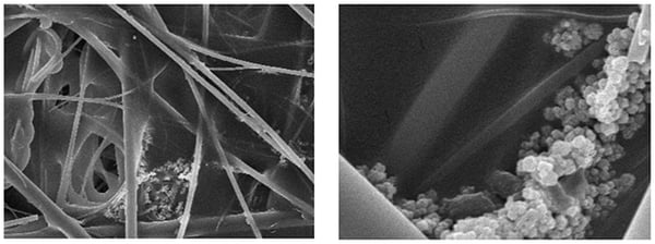
It’s well established that particles can negatively impact semiconductor manufacturing performance. Chemical manufacturers have an opportunity to improve product quality by reviewing their contamination control strategy and aligning with their customers' best practices. The industry standard approach has been to proportionately improve filtration performance as technology nodes advance. Filtration is an effective tool in general, Figure 2, but a one-size fits all approach to filtration is insufficient as new contaminants pose new threats, and our ability to detect new contaminants is challenged. Because metals, ions, particles, and organic extractables can be added to a clean material from interactions with components along the chemical delivery pathway, optimizing your contamination control management approach requires evaluating the materials of construction along the pathway, as well as the components’ interactions with the chemicals being processed. Filters should be selected to remove the contaminants of interest, avoid detrimental interactions, and meet lifetime requirements for a manageable cost of ownership.
 |
Watch members of Entegris’ applications engineering teams discuss the challenges and opportunities for chemical manufacturers.
Collaboration between semiconductor fabs, chemical suppliers, and component suppliers creates a conduit to examine the defect sources and make adjustments to meet wafer yield, device performance, and electronic system reliability requirements, while also improving cost of ownership for each member of the value chain.
To learn more, read The Fight for Purity in Chemical Manufacturing and Clean Chemical Delivery.


