
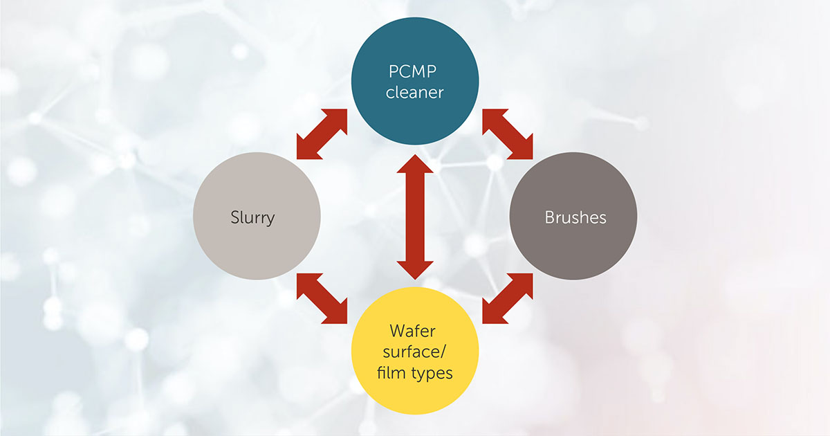
The purpose of a CMP process is simple – to planarize the top layer of oxide or metal with an abrasi...

Science that is transforming lives and enabling the future
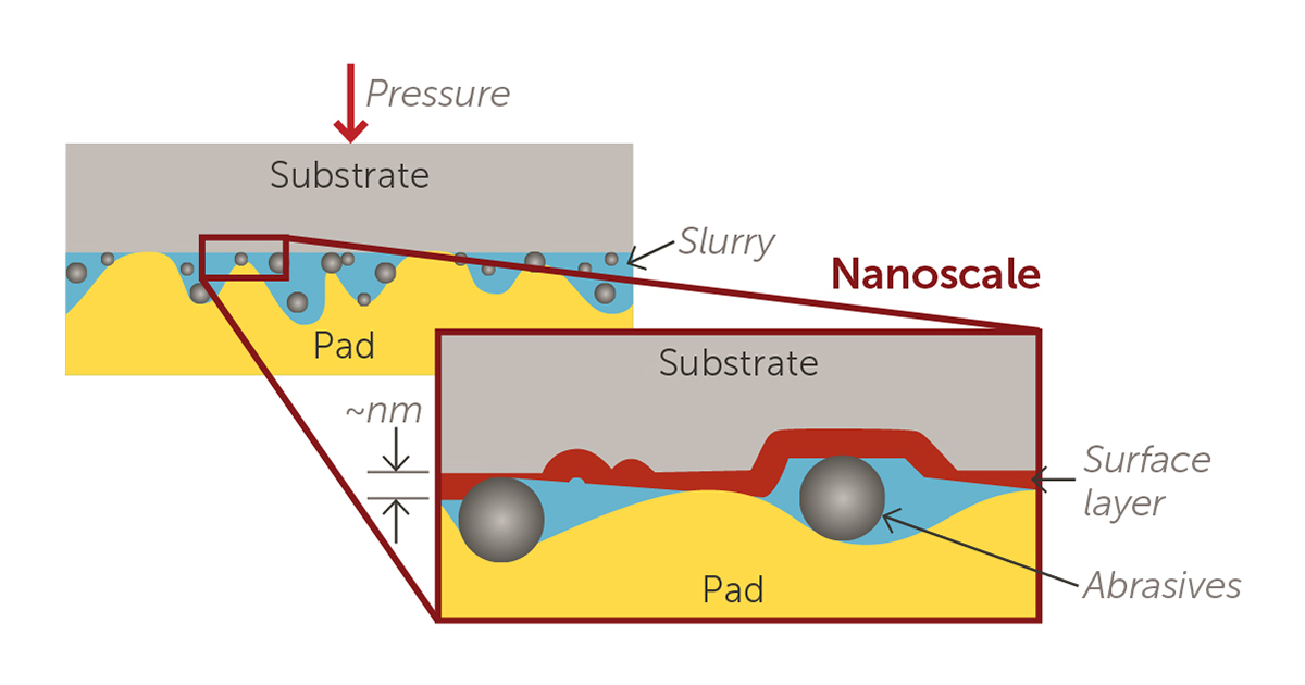
The purpose of a CMP process is simple – to planarize the top layer of oxide or metal with an abrasive slurry. Manufacturing the slurry to the exacting standards required by the end user is not easy. To effectively planarize the wafer surfaces, both large and small abrasive particles must be removed prior to being dispensed. Thus, the target is a narrow particle size distribution between 30 and 200 nm to prevent both microscratches and underlayer defects.
Like all reticles, those used for EUV lithography rely on reticle pods for safe storage and to protect them during lithographic patterning, inspection, cleaning, and repair.
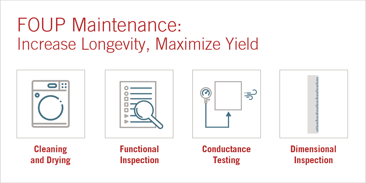
Simplify your operations and supply chain with a versatile contamination control strategy.
Overview The rapid increase of semiconductors in cars enables significant safety, connectivity, mobility, and sustainability improvements. As transportation transforms from being driver controlled to software controlled, automakers must look closer at their ability to measure and maintain product reliability throughout the vehicle’s lifetime.
Electronic devices now serve as the backbone of modern vehicles and have become the focus of quality standards that ensure automotive functional safety. As automakers transform their organizations to adapt and become experts in manufacturing digital machines, current gaps in how the automotive and semiconductor supply chains interact have emerged.
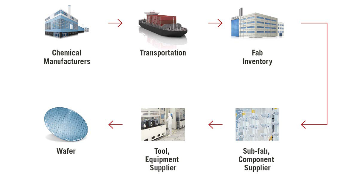
A high purity sub-fab serves as the central nervous system of a semiconductor cleanroom. It houses chemical delivery, purification, recycling, and destruction systems. The sub-fab is where potentially hazardous aqueous chemistries and gases are stored and handled until they are delivered to the cleanroom process equipment located either in the floor above it or the building adjacent to it.
One of the longest held beliefs in semiconductor manufacturing is that yield is the single most important factor in overall wafer processing costs. Even incremental yield increases can significantly reduce manufacturing cost per wafer, or cost per square centimeter of silicon. As such, yield improvement is critical to any successful semiconductor operation. As semiconductor device nodes continue to scale, and 7 nm lines are ramping to production, this belief continues to ring true.
Shrinking feature size, advances in interconnect metals, and the need for ever tighter defectivity control all point to the growing importance of chemical mechanical planarization (CMP) to optimize fab yields. More layers of each chip require CMP to achieve planarity specifications, and contamination must be kept to a minimum.
The Fourth Industrial Revolution is surrounding us with extraordinary technologies that did not exist a few years ago. Autonomous vehicles are already being tested on public streets. Drones range from simple adolescent playthings to short- and long-range military and civilian purposes like surveying landforms, shooting movies, and delivering packages. Vast amounts of video content, created by professionals and amateurs alike, are being filmed, streamed, and stored. Surveillance, both fixed and mobile, is becoming commonplace, server farms are bigger than ever, and 4G networks are being supplemented or replaced with 5G. What all these trends have in common is that they generate enormous amounts of data that must be processed, transported, and stored faster and more reliably than ever before.
The electric vehicle (EV) market is expanding in response to customer demand, with multiple major automotive companies offering lower cost models with longer driving range.
Migration from 2D to 3D structures for high-density memory devices changes the nature of etching and deposition processes, especially as the number of layers for 3D NAND integration grows to 96 and beyond, and new process chemistries become commonplace. The greater number of lengthy processing steps and high aspect ratio (HAR) features involved place new demands on all steps of the chip manufacturing process, including etching, deposition, and cleaning equipment. Consistent process stability becomes harder to achieve.
Most equipment and process engineers become experts at analyzing a wafer map to quickly identify signatures indicating when their equipment or process was the perpetrator of a maverick yield event. But as defect signatures become more subtle and harder to quickly identify, there is a significant need to consider not just what in-line inspection systems are identifying, but specifically what they are not identifying.
The purpose of a CMP process is simple – to planarize the top layer of oxide or metal with an abrasi...
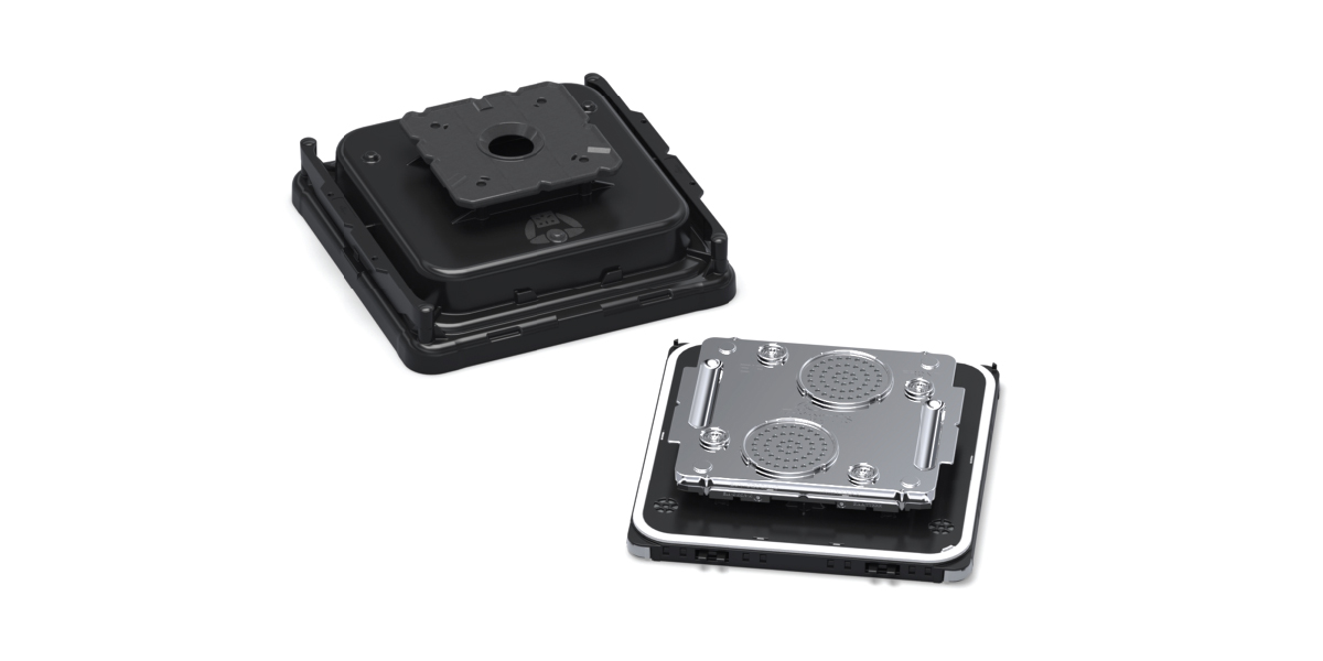
Like all reticles, those used for EUV lithography rely on reticle pods for safe storage and to prote...

Simplify your operations and supply chain with a versatile contamination control strategy.

Overview The rapid increase of semiconductors in cars enables significant safety, connectivity, mobi...

Electronic devices now serve as the backbone of modern vehicles and have become the focus of quality...

A high purity sub-fab serves as the central nervous system of a semiconductor cleanroom. It houses c...
One of the longest held beliefs in semiconductor manufacturing is that yield is the single most impo...
Shrinking feature size, advances in interconnect metals, and the need for ever tighter defectivity c...
The Fourth Industrial Revolution is surrounding us with extraordinary technologies that did not exis...
The electric vehicle (EV) market is expanding in response to customer demand, with multiple major au...
Migration from 2D to 3D structures for high-density memory devices changes the nature of etching and...
Most equipment and process engineers become experts at analyzing a wafer map to quickly identify sig...
© 2026 Entegris. All Rights Reserved

