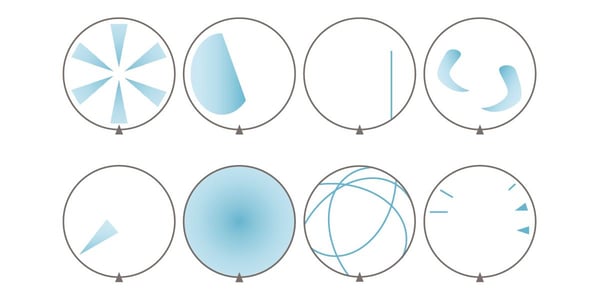
Most equipment and process engineers become experts at analyzing a wafer map to quickly identify signatures indicating when their equipment or process was the perpetrator of a maverick yield event. But as defect signatures become more subtle and harder to quickly identify, there is a significant need to consider not just what in-line inspection systems are identifying, but specifically what they are not identifying.

There is a significant opportunity cost in chasing after weak signatures without ever identifying their root cause. It is now increasingly important to design equipment and processes to be contamination tolerant, providing a robust contamination management strategy to eliminate defects that negatively impact yield and long-term reliability for each process step.
Equipment is designed for optimal performance with the known process gases in use at that particular time. As semiconductor manufacturers extend the useful life of their expensive unit process equipment, the equipment materials of construction may not always be compatible with newly introduced process gases.
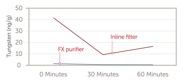
Tungsten removal from HF

As such, changing to a new process gas without first examining compatibility with the materials of construction along the delivery path of your process gas could lead to corrosion and defectivity. For example, hydrogen fluoride gas is very aggressive toward 316L stainless steel, and corrosion is accelerated by the presence of moisture, which in turn can increase the release of volatile metals. While a filter can protect against particles in a gas stream, it cannot remove moisture and cannot protect against corrosion. By introducing a purifier into a hydrogen fluoride stream, both moisture and tungsten can be removed, increasing the purity of the gas stream significantly.
Conclusion
As defectivity sensitivity increases and the size of a critical defect dramatically decreases, it is increasingly important to creatively collaborate across the supply chain to identify and mitigate contamination. No single material supplier, equipment maker, fab, or semiconductor customer alone has the required insight across the semiconductor manufacturing ecosystem, nor does each entity have the time or resources to pursue all solutions. It is only by collaborating across the value chain to develop new techniques that identify, characterize, and mitigate contamination that we can achieve the most effective, holistic contamination control that addresses both the defects we can see and those we have yet to see.
To read the full paper including five case studies visit www.entegris.com/defectivity


