

The drive for ever more powerful microprocessors and greater memory storage places demands on all steps of the semiconductor wafer fabrication process. At some point, incremental improvements are no longer sufficient, and further device shrinking requires a completely different technology. The semiconductor industry is now experiencing this with lithography, where extreme ultraviolet (EUV) lithography is replacing 193 nm immersion (193i) lithography for more and more critical chip layers.
Once device dimensions shrink beyond a specific point, line width and spacing approach the resolution limits of 193i lithography. Because of its shorter wavelength, EUV lithography enables a streamlined process that extends single exposure lithography beyond what is possible with 193i. By delaying the need for implementing self-aligned double patterning (SADP) or self-aligned quadruple patterning (SAQP) to achieve the required CD (critical dimension) or pitch, EUV can break through the cost and yield barriers of 193i at advanced nodes. The tipping point appears at the 5 nm node for logic and the 1a node for DRAM devices.
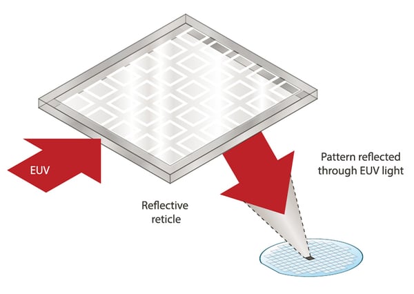 Figure 1: EUV lithography process with a reflective reticle
Logic devices at the 7 nm node can still get by with 193i lithography by making extensive use of SADP. Of the 50 masks used to make a chip, around half of them require multi-patterning. Leading manufacturers are, however, implementing EUV on select layers of some 7 nm devices to reduce the number of layers requiring SADP.
At 5 nm, 193i lithography becomes too costly. Designs would need to resort to multi-patterning on many more layers to achieve the required dimensions with 193i lithography, pushing the total number of process steps to an unsustainable level. In addition, double patterning is not sufficient. Quadruple patterning can achieve the desired resolution, but most designers prefer to avoid it because of its complexity. With each chip requiring up to 50 patterned layers, the cumulative effect on yield is a problem. Misalignment is a serious concern. Single patterning with EUV is much less risky and cost effective, requiring only 10 separate process steps for each mask compared to 120 for SAQP.
For even more advanced nodes, EUV will enable manufacturing that would not even be possible with 193i lithography.
While the concept of EUV lithography is not new, the technology is now realizing its potential to become widespread for commercial production of logic and memory devices. Major manufacturers are using EUV lithography for volume production of advanced logic devices now. But even though the technology is in production, there are hurdles to overcome.
Fabs, OEMs, and equipment and materials suppliers all need to work together to improve process control. Yield improvement will become the number one issue in every EUV-enabled design, and the industry must take steps to solve the inherent defect challenges. Advances in EUV lithography must address three key challenges:
- Reducing contamination from the reticle to control defect levels,
- Improving photoresist technology to create a more robust process, and
- Extending EUV through advances in scanner hardware.
We invite you to download our new white paper: EUV Enablement: Solving defect challenges in the EUV process to see why these advances are necessary for the success and expansion of EUV lithography.

