

NEW PARADIGMS IN MATERIALS DEPOSITION FOR BOTH LOGIC AND MEMORY DEVICE MANUFACTURING
We live in an increasingly connected world that has developed an almost unquenchable thirst for data. To process this raw data into something that is actionable requires the most advanced artificial intelligence (AI) chips for a multitude of applications, from machine learning and autonomous vehicles, to smart cities and efficient energy sources. The quest to develop these devices is driving integrated device manufacturers (IDMs) to push semiconductor manufacturing technology to
its very limits.
Some IDMs continue chasing node scaling beyond 10 nm to 5 nm and even 3 nm, while others are abandoning planar architectures and focusing efforts on complex, three-dimensional (3D) structures for both logic and memory devices.
Scaling to smaller device nodes and creating vertical structures is driving completely new paradigms in materials deposition for both logic and memory device manufacturing. Requirements for deposited film conformality are driving changes in process technology from chemical vapor deposition (CVD) towards pulsed CVD and atomic layer deposition (ALD). At the same time, new methods for developing and qualifying customized deposition materials that meet the needs of IDMs and the steps required for ramping to high-volume manufacturing (HVM) are needed.
THE TRANSITION FROM CVD TO ALD
Thin-film deposition is a cornerstone process for integrated circuit (IC) device fabrication. CVD is the most used method for thin-film growth. In CVD, precursors and reactants are mixed in the process chamber and delivered in a steady state to form a film on the wafer.
In ALD, the precursor and reactants are delivered alternately in pulses to create temporally distinct half-reactions. While ALD is a slower process than CVD, it is more tunable and can be more precise. In this way, film deposition is well controlled and provides the greatest level of thin-film conformality, which is required for complex
3D structures.
A hybrid approach that is being adopted in semiconductor manufacturing leverages the speed of CVD and precision of ALD. Referred to as pulsed CVD, it involves the pulsed delivery of the precursor while the co-reactant is flowed into the process chamber in a continuous manner. The resulting conformality of the deposited thin-film mimics those formed by the ALD process.
THERMALLY DRIVEN PRECURSOR MOLECULES
Developing precursor molecules for CVD and ALD that are well suited for conformally coating the tight pitches and high aspect ratios of 3D structures is critical for both logic and memory.
Although plasma processes are often used for device fabrication, the utilization of plasma-enhanced (PE) processes, such as PECVD and PEALD, is becoming more challenging to implement, especially where complex 3D structures are concerned.
Depositing films that possess uniform composition and con-formality, as well as uniform material and electrical properties, increasingly requires thermally driven processes, rather than plasma-based, thin-film deposition processes (Figure 1).
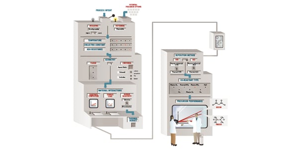
Figure 1. The precursor toolbox works like a decision tree, inputting design challenges associated with silicon semiconductor fabrication process steps. Each of the toolbox inputs can be compared to pre-screened results, revealing a qualified short list of precursor candidates and supporting recommendations for the deposition process. |
FROM PATHFINDING THROUGH HVM: A STEP-BY-STEP APPROACH
Unlike other process materials, advanced deposition materials (ADMs) produce a
thin film that stays in the working IC and therefore must meet lifetime and accelerated testing requirements. Furthermore, the successful development of
ADMs and their processes requires careful collaboration between the integrated device manufacturer (IDM), the original equipment tool manufacturer (OEM), and
the precursor material supplier.
This collaborative journey begins with the IDM’s problem statement and the requirements for the proposed solutions. The process then continues through pathfinding, concept and feasibility (C&F), customer demos, development, device integration, and finally the ramp to high-volume manufacturing
(HVM). Done correctly, the entire process from start to finish can take anywhere
from one to four and a half years, broken down as follows:
- One to three years for pathfinding, C&F, demos, development, and initial integration
- Eighteen months for ramp to HVM
CONCLUSION
Meeting the challenges of future device nodes and complex 3D structures requires innovation, creativity, and inter-company collaboration. A holistic and iterative approach toward new product development is the preferred way to manage the development of precursors for next-generation ALD and CVD processes. This means working collaboratively with both IDMs and OEMS in a very fast-paced and competitive environment. New materials development, as well as packaging, transport, and delivery system optimization must all be considered.
Furthermore, the development of new ALD and CVD materials, new processes, and new equipment must be developed simultaneously. The new paradigm calls for careful and rapid pathfinding, thorough C&F steps, and a detailed approach to HVM ramping and quality control. This winning combination of iterative product development in a collaborative mode is a recipe for successful next-generation, industry-leading innovation.
> Explore how through close collaboration, Entegris provides reliable, extremely high-purity materials to solve the most advanced technology challenges.

