The electric vehicle (EV) market is expanding in response to customer demand, with multiple major au...

Science that is transforming lives and enabling the future
The electric vehicle (EV) market is expanding in response to customer demand, with multiple major automotive companies offering lower cost models with longer driving range.
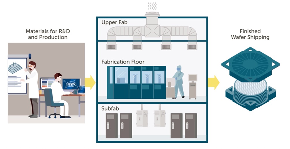
Most equipment and process engineers become experts at analyzing a wafer map to quickly identify signatures indicating when their equipment or process was the perpetrator of a maverick yield event. But as defect signatures become more subtle and harder to quickly identify, there is a significant need to consider not just what in-line inspection systems are identifying, but specifically what they are not identifying.
The drive for ever more powerful microprocessors and greater memory storage places demands on all steps of the semiconductor wafer fabrication process. At some point, incremental improvements are no longer sufficient, and further device shrinking requires a completely different technology. The semiconductor industry is now experiencing this with lithography, where extreme ultraviolet (EUV) lithography is replacing 193 nm immersion (193i) lithography for more and more critical chip layers.
NEW PARADIGMS IN MATERIALS DEPOSITION FOR BOTH LOGIC AND MEMORY DEVICE MANUFACTURING We live in an increasingly connected world that has developed an almost unquenchable thirst for data. To process this raw data into something that is actionable requires the most advanced artificial intelligence (AI) chips for a multitude of applications, from machine learning and autonomous vehicles, to smart cities and efficient energy sources. The quest to develop these devices is driving integrated device manufacturers (IDMs) to push semiconductor manufacturing technology to its very limits.
Entegris recently wrapped up an exciting week at the first-ever SEMICON West virtual event. The event provided a great opportunity to connect with the community and gain valuable insight into the future of the industry.
Photochemicals are playing an increasingly important role in bringing next generation devices to reality. While semiconductor manufacturing has always needed a pure, contamination-free environment, the requirements are tightening even further.
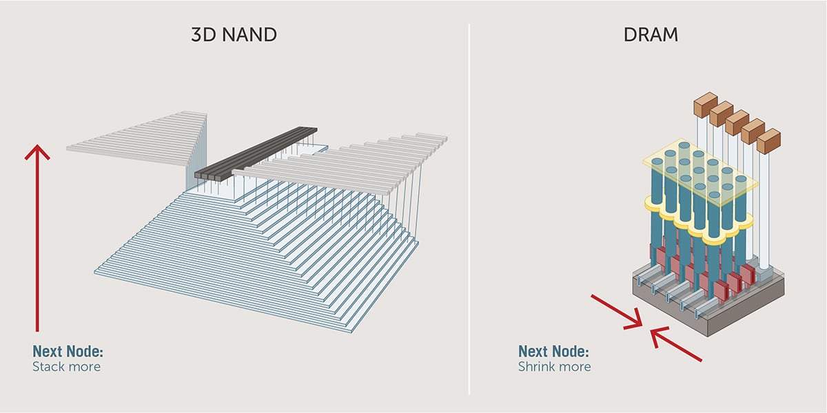
DRAM architecture has remained virtually unchanged for the past decade, with the dimensions shrinking proportionally with each successive device node. This linear path, however, is reaching its limits for nodes below 20 nanometers (nm) including 1x, 1y, 1z, 1a, and 1b. A major change will be needed soon if DRAM is to keep up with advances in logic.
The rapid increase of semiconductors in cars enables significant safety, connectivity, mobility, and sustainability improvements. The standards to measure reliability under the tough conditions a car presents are based on how vehicles operate today. Conventional vehicles are generally idle 95% of the time. As a result, the expected lifetime of the electronics systems is well beyond the lifetime of the vehicle itself.
The automotive supply chain is transforming with the development of autonomous vehicles. The rise of electronic systems leads designers and manufacturers to seek collaboration partnerships. Antoine Amade, senior director EMEA/NA sales, was recently interviewed by SEMI to discuss the zero-defect challenges facing semiconductor fabs and the expansion of the GAAC (Global Automotive Advisory Council).
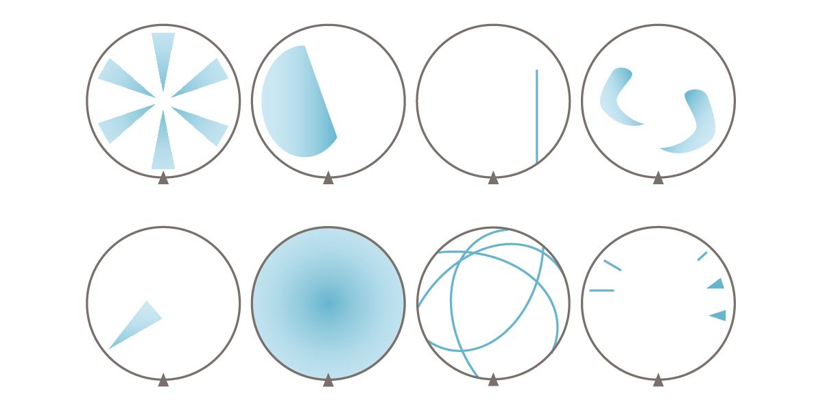
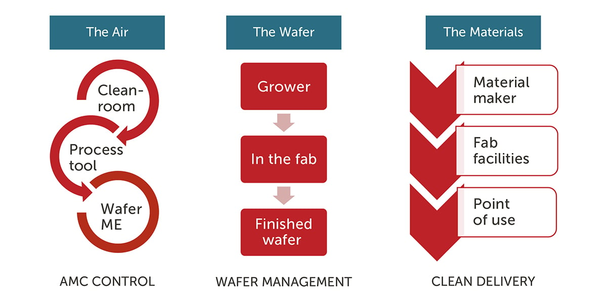
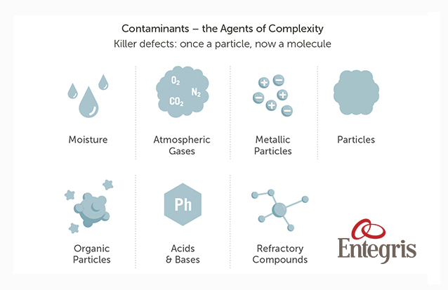
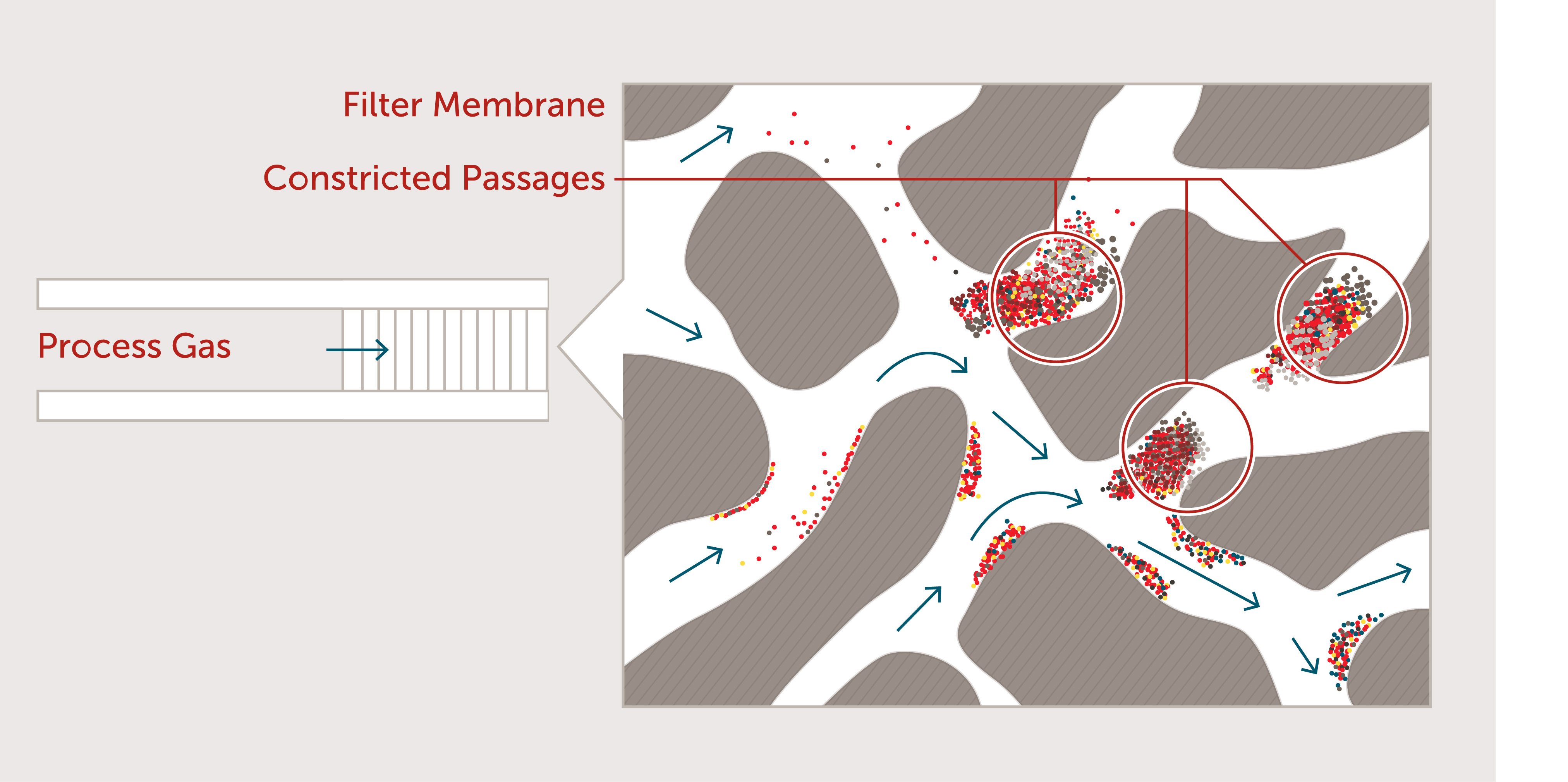
During the semiconductor manufacturing process, contamination can be introduced from the air, equipment, cleanroom personnel, process water, process chemicals, and process gases.1 Careful identification of the contaminant source is required to best identify mitigation strategies that utilize filtration. Installing a filter can reduce defectivity, but this mitigation strategy will not indefinitely protect a gas stream from contamination.
The desire for ever more computing power in a smaller footprint requires transistors that perform faster while consuming less power. However, new materials and architectures developed with these goals in mind are not easy to transfer from research and development to full-scale, high-volume production.
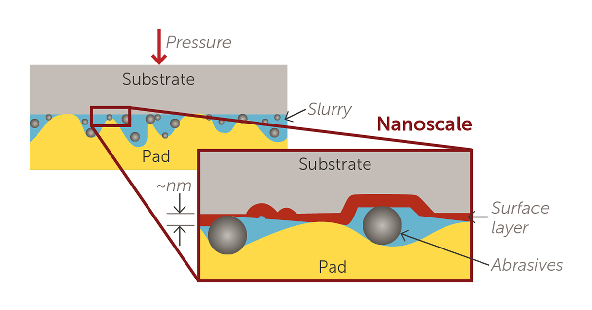
Dewetting and non-dewetting are not common terms used every day, yet are vital to the functionality of liquid filters.
The electric vehicle (EV) market is expanding in response to customer demand, with multiple major au...
Most equipment and process engineers become experts at analyzing a wafer map to quickly identify sig...
The drive for ever more powerful microprocessors and greater memory storage places demands on all st...
NEW PARADIGMS IN MATERIALS DEPOSITION FOR BOTH LOGIC AND MEMORY DEVICE MANUFACTURING We live in an i...

Entegris recently wrapped up an exciting week at the first-ever SEMICON West virtual event. The even...

Photochemicals are playing an increasingly important role in bringing next generation devices to rea...
DRAM architecture has remained virtually unchanged for the past decade, with the dimensions shrinkin...
The rapid increase of semiconductors in cars enables significant safety, connectivity, mobility, and...
The automotive supply chain is transforming with the development of autonomous vehicles. The rise of...
During the semiconductor manufacturing process, contamination can be introduced from the air, equipm...
The desire for ever more computing power in a smaller footprint requires transistors that perform fa...

Dewetting and non-dewetting are not common terms used every day, yet are vital to the functionality ...
© 2026 Entegris. All Rights Reserved

