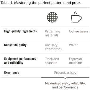
In the early days of semiconductor manufacturing, fabs would remove contaminants from their process fluids in a sequence that could be analogized to making a cup of coffee. By using a filter with tiny pores, large contaminants (coffee grounds) are separated from water. Because the coffee grounds are too large to pass through the filter, they can’t pass into the coffee we drink.
 As semiconductor features have become smaller and more geometrically complex, they’ve also become sensitive to smaller and more diverse contaminants. This presents a problem for traditional contamination control methods. To extend the analogy, imagine that the incoming water quality has changed, and you need to remove both the grounds and trace contaminants that will affect the taste of the coffee.
How do you remove the contaminant without removing the caffeine or flavors unique to the coffee bean? This could be done by using a combination of removal mechanisms in filters and purifiers.
Finer Sieves Aren’t the Solution for All Contaminants
Earlier filtration products approached the problem of smaller contaminants by essentially making filters with smaller pores. This method is known as size exclusion – it lets small particles through while screening large ones out.
Smaller and more complex semiconductors can be disrupted by molecular contaminants such as dissolved metals and organics. Dissolved metals, for example, require a different removal mechanism to prevent them from contaminating a wafer.
What this means is that the semiconductor industry requires additional methods of filtration to ensure the quality and reliability of their products. Instead of filtration alone, these new methods fall under the heading of purification. Purification methods can be tailored for specific contaminant removal needs.
What’s the Alternative to Size Exclusion?
Purification relies on adsorption, which effectively means creating a membrane or media that’s designed to remove specific contaminants based on their chemical properties instead of physical size. For example, let’s say that analysis of a solvent reveals the presence of metals that will compromise a pattern. One would mitigate this contaminant by introducing a material that attracts this metal without interacting with the other elements in the patterning material.
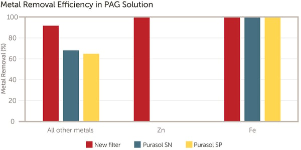
 Figure 1. Targeted removal mechanisms align to contaminant affinity
One advantage of adsorption media is that they can be tuned to target specific contaminants. By altering the chemistry of the membrane or media, you can target contaminants more precisely than by using a mechanical filter. Because materials encounter unique delivery, storage, and mixing conditions from the point of manufacture to wafer dispense, they need tools to mitigate unique contaminants and sensitivities.
Targeted removal enables manufacturers to install filters and purifiers in unique combinations that are specifically designed for their individual chemistries.
Micro Contamination Control for Increasingly Sensitive Chemistries
While size exclusion filtration may be an excellent choice for making a cup of coffee, it’s no longer viable on its own for the needs of semiconductor manufacturing. As the industry explores increasingly smaller dimensions and more complex chip design geometries, it needs to mitigate increasingly smaller and more diverse contaminants.
Use of both size exclusion and adsorption contaminant removal mechanisms are increasingly effective at addressing the volume and diversity of today’s semiconductor materials. Using an approach that’s tailored to the customer, targeted removal can mitigate these contaminants wherever they occur.
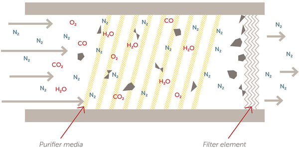
 Figure 2. Gas purifier removal mechanisms.
For more information about Entegris and our targeted removal approach, visit our resource center today.


