Silicon carbide (SiC) has become popular with chipmakers. Its wide-bandgap structure offers many design benefits for the operations of power semiconductors. Compared to silicon, SiC wafers enable the fabrication of faster, more efficient devices that can both operate at higher temperatures and remain stable when deployed in extreme temperature environments. Processing SiC wafers using the same materials and methods as silicon wafers is not a viable option, however.
Chemical mechanical planarization (CMP) is vital to high-volume chip production, and compound semiconductors like SiC are no exception. However, the SiC manufacturing process, as well as the material itself, pose some key challenges for CMP. These must be addressed to achieve chipmakers’ yield and throughput objectives.
Planarizing SiC Without Exaggerating Defects
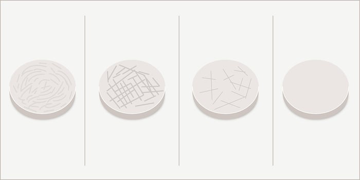
Let’s look at a few of the primary potential defect sources that must be mitigated – starting with CMP itself. Because CMP processes involve abrasion and debris removal, they can aggravate surface and sub-surface defects generated during SiC wafer growth and creation. Once the SiC wafers are created, they are sawn, ground, and lapped. Next, the wafer is prepared for material deposition using CMP. Each of these initial steps can create defects that degrade both device performance and overall wafer yield.

Figure 1. Preparing the Silicon Wafer
Surface defects such as scratching, pitting, and particle agglomeration can’t be removed from the wafer. This means that CMP processes must be performed with precision and accuracy so that the SiC wafer surface is polished without these defects being exposed or exacerbated. This makes selecting the right CMP slurry, pads, and process parameters vitally important.
Optimizing Slurry for SiC CMP
CMP slurry typically consists of abrasive nanoparticle powder dispersed in a chemically reactive solution. Its purpose is to remove a thin layer of metal or oxide using a combination of abrasive particles and chemical additives. Using high-performance slurries for wafer polishing enables scalable manufacturing of smooth, defect-free SiC wafers – improving material performance by as much as 50%.
While the slurry is the most critical part of the CMP process, the pad must be compatible with the slurry. This is the only way to achieve the desired planarity while also preventing scratches or contamination of the SiC wafer surface. Investigation of different pad materials indicates that thermoplastic polyurethane CMP pads perform far better than traditional thermoset polyurethane pads. They can minimize surface damage while optimizing removal rates due to bulk hardness.
Time is Money – Optimizing Material Removal Rates for SiC
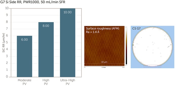
This brings us to another key challenge that SiC poses for CMP – low material removal rate (MRR). SiC, by nature, is dense, chemically inert, and harder to planarize than silicon. SiC-optimized slurries repeatedly create and then remove a nanoscale layer to create a smooth surface. The slurry particles must be the right size and hardness to remove only the oxidized layer – going too deep will create scratches, compromising the quality of the polishing process.

Figure 2. Multi-faceted solutions approach yields class leading material removal rate (MRR), surface roughness below 1.5A, and ultra-low defectivity (no scratches)
Speeding the rate of removal for the oxidized layer uses less slurry. It also means that manufacturers can polish the same number of wafers in a shorter time. By selecting the right CMP partner with the necessary expertise and an arsenal of pads and slurries, the SiC device maker can achieve an advanced material removal rate of 5 microns per hour or more. They can also monitor particle counts and sizing to make sure filtration and other process conditions are optimized.
While defectivity, MRR, and slurry optimization are primary issues for SiC manufacturers, the challenges don’t stop there. For example, manufacturers also need to mitigate the impact of ex-situ conditioning while lowering total cost of ownership.
Visit Silicon Carbide (SiC) CMP Solutions to learn more about all the key process challenges CMP poses for SiC manufacturing and how these challenges are being addressed – including several aggregated real-world customer examples. You can also read our white paper, “Solving CMP Challenges in High-Volume SiC Production,” and watch our webinar, “Advanced CMP of Silicon Slurry for EVs and Power ICs.” Contact the Entegris team to collaborate on your SiC solutions.


