

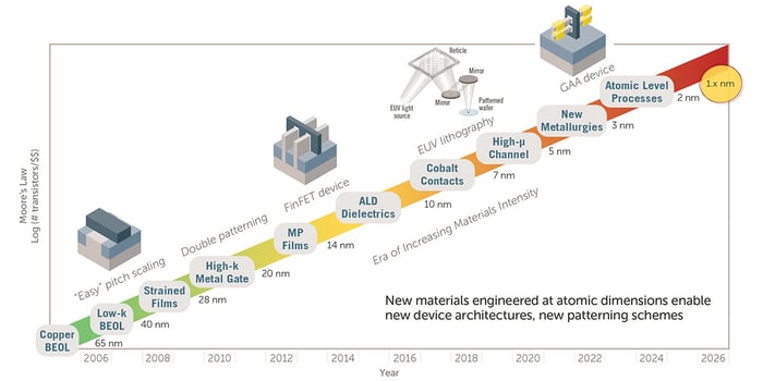
For decades, the semiconductor device manufacturing mantra was “How do we make them smaller, cheaper, and faster?” The pursuit of Moore’s Law – the doubling of transistors on a chip every two years – was achieved through planar scaling. But that approach could only go on for so long. The mantra now is “How do we improve power, performance, area, and cost (PPAC)?” At the 14 nm node, it was clear that the best way to push the limits of semiconductor device PPAC was to take it into the third dimension.
Fin field-effect transistor (FinFET) devices were the industry’s first foray into the third dimension. Since then, we’ve seen exploration and development of gate-all-around (GAA) structures, forksheets, and complementary FETs (CFETs) as we move down the node scale from 3nm and beyond. The commonality of all these novel nanostructures is the increasing complexity and aspect ratio of 3D structures in logic, DRAM, and NAND flash.
Building 3D nanostructures poses holistic challenges to almost all semiconductor processes, including etch, deposition, implant, and cleans. The combination of finer features and high aspect ratios makes surface reactions a dominating factor because of an increase in surface-area-to-volume ratio. The unconventional physical and chemical behaviors of chemical species in these complex 3D nanostructures further complicates the chemical reactions. This has had an enormous impact on process chemistries and gases used, as formulations must now be tuned at the molecular level to achieve desired performance results.
For example, etch chemistries must be carefully formulated and processes timed to avoid redepositing silicon back onto the nanostructure which can form defects. The same goes for cleans formulations to effectively remove post-etch residue without corroding exposed metal surfaces and corresponding liner, barrier, or etch stop layers.
No matter how formulations are designed or applied, the key challenge lies in the prediction and validation of their performance within complex nanostructures in targeted applications. Conventional approaches to chemistry formulation are intensive, lengthy, and costly processes involving both chip manufacturers and solutions providers. Additionally, laboratory coupon tests used to test the formulations are not designed to capture the behaviors of formulations developed for 3D nanostructures. Without understanding these behaviors in a test environment, it is difficult to determine how the formulations will perform in high-volume manufacturing, which is the ultimate goal.
There is a better way. At Entegris, we’re using computational chemistry based on density functional theory (DFT) and molecular dynamics (MD) to support the development of chemistry formulations for 3D nanostructures.
DFT is used to investigate the local properties of a very small system of only a few particles based on their electronic structures. However, DFT alone does not describe the intermolecular interactions that are critical to understanding chemical reactions of materials on 3D nanostructures.
MD is used to analyze the physical movement of particles (atoms or molecules) based on the force field between them over a fixed period to provide a dynamic view of the system’s evolution. By implementing MD for modeling and simulation, we can calculate the macroscopic physical or chemical properties of formulations to understand their behaviors on 3D nanostructures.
When used in concert, MD complements the DFT and continuum models, and it also works with the two synergistically to extend the scope of applications in various areas of interest. In this way, we’re using MD to bridge conventional quantum mechanics’ DFT and rule-based continuum models already in place at Entegris.
To learn more about how Entegris is solving materials challenges for building 3D nanostructures, read the article “Embedding Computational Chemistry in Material Development: Applications of Molecular Dynamics on Formulation Design for Complex HAR 3D Nanostructures” in our 2022 Scientific Report.

