
Silicon Carbide’s Next Phase: From Expansion to Optimization

Science that is transforming lives and enabling the future
Silicon Carbide’s Next Phase: From Expansion to Optimization
Sustainability Challenges Around SiC Polishing Slurry recycling supports cleaner semiconductor manufacturing
Empowering Semiconductor and Device Performance with Improved Point-of-Use Filtration
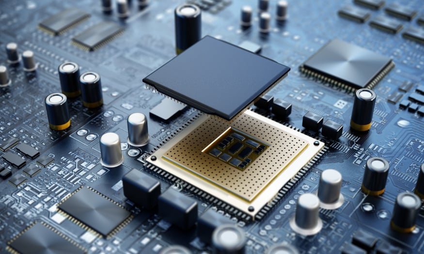
Driving the Future with SiC The semiconductor industry is abuzz with discussions around silicon carbide (SiC) — a material poised to revolutionize power electronics. Global megatrends like sustainability, the rise of electric vehicles, and the growing demands of AI systems have made SiC essential for enabling efficient, high-performance solutions. At Entegris, we’ve embraced this momentum, working with industry-leading chipmakers to help make an impact in the SiC space. Here’s a review of some of our exciting work around SiC over the past year.
Entegris Offers New FOUP Form-Factors for Non-Standard Wafers Over the last few years, 3D stacking has gone from a relatively niche fabrication method to an absolute necessity for cutting-edge applications. As chipmakers delve into smaller and smaller nodes, stacking and die-bonding wafers has become a preferred way of creating more processing power in a smaller space. Stacked and bonded wafers don’t behave the same way as 2D wafers: Wafers are thinned prior to bonding, which results in wafers that can sag when handled Bonded wafers are thicker and heavier than 2D wafers when assembled Bonded wafers can also warp following assembly Many automation tools rely on the predictable geometry and characteristics of 2D silicon wafers for safe handling and transport. While stacked and bonded wafers are a game-changer for miniaturization, they can also force manufacturing compromises unless chipmakers adopt specialized tools for the back end of the line (BEOL).
Entegris ESD Valves, Fittings, and Tubing: An Introduction
Gas Purifier Regeneration: Putting Circularity into Practice
Hydrogen composes about 75% by mass of the normal matter in the universe, existing as H2 gas under standard conditions. This abundance of supply creates opportunities in numerous applications, including semiconductor manufacturing, for which hydrogen is considered a bulk gas and is employed in many parts of the ecosystem.
Changing one material in the semiconductor manufacturing process has a cascading effect on multiple process steps. Consider the replacement of tungsten (W) and copper (Cu) with molybdenum (Mo). Integrated device manufacturers (IDMs) are implementing Mo in advanced designs, focusing on 2-nanometer (nm) nodes and below. Mo is highly conductive, can be deposited without a titanium or titanium nitrid
Silicon carbide (SiC) has become popular with chipmakers. Its wide-bandgap structure offers many design benefits for the operations of power semiconductors. Compared to silicon, SiC wafers enable the fabrication of faster, more efficient devices that can both operate at higher temperatures and remain stable when deployed in extreme temperature environments. Processing SiC wafers using the same materials and methods as silicon wafers is not a viable option, however.
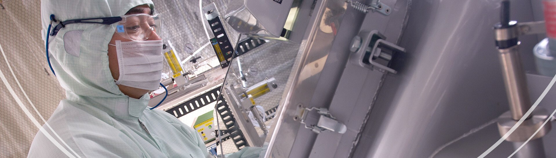
If you asked a semiconductor process engineer to name their biggest challenge when tackling the next technology node, they would likely tell you it is figuring out how to achieve high device yields. This is mainly due to an increase in possible points of contamination as the number of potential contaminants grows and their sizes shrink. It is becoming particularly difficult to detect metal contaminants and pinpoint their root cause so they can be eliminated. That’s because they can form anywhere in the process flow.
Silicon Carbide’s Next Phase: From Expansion to Optimization

Sustainability Challenges Around SiC Polishing Slurry recycling supports cleaner semiconductor manuf...
Looking Back at 60 Years of Moore’s Law

Empowering Semiconductor and Device Performance with Improved Point-of-Use Filtration

Driving the Future with SiC The semiconductor industry is abuzz with discussions around silicon carb...
Entegris Offers New FOUP Form-Factors for Non-Standard Wafers Over the last few years, 3D stacking h...

Entegris ESD Valves, Fittings, and Tubing: An Introduction
Gas Purifier Regeneration: Putting Circularity into Practice

Hydrogen composes about 75% by mass of the normal matter in the universe, existing as H2 gas under s...
Changing one material in the semiconductor manufacturing process has a cascading effect on multiple ...

Silicon carbide (SiC) has become popular with chipmakers. Its wide-bandgap structure offers many des...

If you asked a semiconductor process engineer to name their biggest challenge when tackling the next...
© 2026 Entegris. All Rights Reserved

