

Things are not always as they appear. Take semiconductor manufacturing. On the surface, it may seem that the secret to making semiconductor devices more advanced lies in the design. But just as an architect’s design for a building may not be structurally feasible without the right materials, a semiconductor device design may not be functional if the materials and their interactions are not considered and optimized.
To truly optimize semiconductor manufacturing processes, we must take into consideration every interaction that occurs at each surface. Every step along the way requires a deep understanding of surface science — from the silicon wafers themselves to the additive and subtractive processes used in advanced IC fabrication and the delivery pathways for all the chemistries needed for those unit processes.
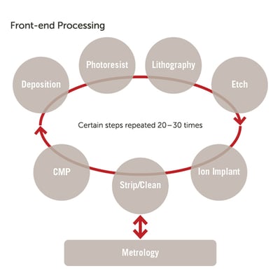 Surface science specifically refers to the study of the chemical and physical processes that occur at the interface between two solids or between a solid and either a liquid or a gas. Today’s most advanced chips contain tens of billions of transistors, each with critical, nanometer scale features. Such miniaturization requires the uniform deposition and selective removal of material at atomic scale dimensions. A plethora of specialized chemistries and gasses are involved in etch, deposition, and planarization processes, all of which are designed to change the surface of the wafer. The finer the features, the greater the impact of interface incompatibility and possible contamination sources.
The impact of surface science extends to how these chemistries and gasses are delivered to semiconductor process tools. For example, the polymeric materials used to manufacture storage and shipping containers, miles of tubing, and hundreds of filters represent thousands of interactions where potential contamination can be introduced. "Therefore, it is not enough to only understand the process chemistries, but also the interactions of those chemistries with the surfaces of the delivery and contamination control systems." A holistic approach would include effectively capturing contaminants that form in the chemistries during delivery and preventing undesirable interactions that could cause contamination.
Another source of potential contamination is carrier gasses, such as nitrogen, that enable the delivery of process chemistries in advanced technologies. Gas and air purification methods that rely on chemisorption and physisorption to capture molecular contaminants are critical for preventing the degradation of process chamber components, such as the mirrors and optics in a photolithography scanner.
Lastly, another capability that is important for contamination control is being able to characterize the surface interface. This can be accomplished with advanced surface metrology that goes beyond standard characterization methods.
Understanding the science at interfaces is the foundation of Entegris’ contributions to enabling advanced technologies in semiconductor manufacturing. Not only do we support surface-science innovation in each of the critical unit process steps, but we also focus our research on end-to-end contamination control to ensure purity throughout the semiconductor manufacturing process.
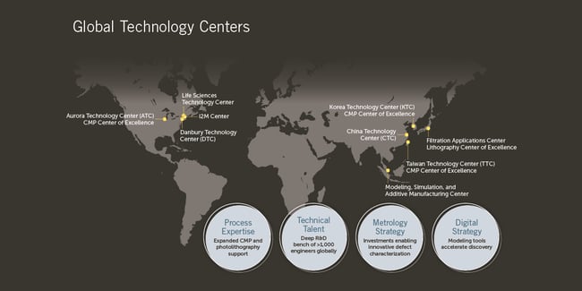
Our worldwide network of technology centers remains at the forefront of key contaminants detection, developing hybrid methodologies for detecting surface contaminants, which drives the design of contamination control solutions that target molecular contaminants.
 For a deeper dive into surface science, including impacts on the semiconductor industry and how Entegris leverages its expertise to meet these challenges, read the article “Introduction to Surfaces and Interfaces” in our 2022 Scientific Report.

