 To wrap up the Year of the Tiger (2022), there are still lessons to be learned from the animal kingdom. A tiger out in the open roaming the savannah is at risk of injuries from predators, including human hunters. Wafers left out in the open in a fab are susceptible to damage that can cause dramatic yield drops. The larger the wafer diameter, the greater the risk.
Back in the 20th century, wafers lived in open cassettes in a fab environment. This arrangement was acceptable when the largest wafers were 200 mm in diameter. Separate transport boxes or pods were available for safer transport between tools. These outer containers were helpful and also a bit cumbersome.
 |
The transition from 200 to 300 mm wafer fabs in the 1990s ushered in a new era of protection needs. Not only were wafers larger and more fragile, but they contained finer and more contamination-sensitive features. It was time for fab transport to evolve.
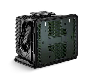
Enter the front-opening unified pod, the FOUP. The migration to 300 mm offered a unique opportunity to completely change how wafers were transported. With Motorola in the lead, the semiconductor industry eventually embraced the new patented design.
FOUPs protect wafers. They offer a clean micro-environment with controlled light, moisture, and oxygen levels. Advanced purge capabilities in today’s FOUPs create uniform airflow and the option to introduce nitrogen as needed.
A well-designed FOUP does not, however, eliminate the risks of wafer damage. A wafer will travel 8 to 16 kilometers as it moves through hundreds of process steps before being diced into individual dies. During that journey, the FOUP experiences wear and tear as it travels in the fab. Deformed gaskets, damaged filters, or microcracks in various FOUP components increase the potential for defects.
For example, corroded metal springs shed metal particles that can deposit on the wafers. Aging door seal gaskets compromise the environment inside the FOUP and increase particle contamination. Both situations reduce wafer yield because the FOUP is no longer doing its job effectively.
If a tiger becomes injured, it can no longer hunt effectively. It needs to recuperate. Tigers and other members of the cat family routinely lick themselves to clean their fur and reduce the chance of infection. Their saliva has antiseptic properties that accelerate healing.
FOUPs, unlike tigers, cannot clean themselves. Routine washing to remove surface particles before each wafer start is part of maintenance. Comprehensive FOUP maintenance goes far beyond cleaning, however. Preventive maintenance includes thorough inspections to identify worn parts, test functionality, and confirm that all dimensions are within specifications. Gaskets, filters, and O-rings require annual replacement. Inspections will determine if any parts are defective and must be replaced sooner than scheduled.
Old FOUPs can be upgraded by adding advanced purge technology. With proper maintenance, FOUPs can last for well over a decade. Eventually, they may need replacement, but it is possible to extend their useful lifetime.
|
|
Investing in FOUP repair, parts replacement, and even replacing older models with the latest designs is worthwhile because it improves wafer yield. Keeping yield high makes the fab more resource-efficient and reduces the total cost per wafer.
Wise tigers know that they need to heal from injury before returning to hunt. Wise fab operators know they must keep their FOUPS in top operating condition to allow their fabs to run with optimum yield.
Are your FOUPs achieving their potential?
Read our white paper, “Yield Advantages Through Maintaining and Upgrading FOUP Populations,” to learn more about how optimum FOUP integrity can improve your bottom line.


