
Silicon carbide (SiC) has become popular with chipmakers. Its wide-bandgap structure offers many des...

Science that is transforming lives and enabling the future
Silicon carbide (SiC) has become popular with chipmakers. Its wide-bandgap structure offers many design benefits for the operations of power semiconductors. Compared to silicon, SiC wafers enable the fabrication of faster, more efficient devices that can both operate at higher temperatures and remain stable when deployed in extreme temperature environments. Processing SiC wafers using the same materials and methods as silicon wafers is not a viable option, however.
Powder can be a mess when not delt with properly. Have you ever dropped a bag of flour on the floor after coming home from the store? Cleaning up the mess is terrible (speaking from experience, don’t add water or you just make glue). Now imagine doing that in a manufacturing suite with powdered media. The powder is literally designed to grow cells, so anything you miss is just a new petri dish that can generate contamination. Plus, there’s the added challenge of having to validate that the room is clean after attending to the spill.
Entegris is delighted to announce our new interactive tool intended to help the life sciences industry better understand how we can support the entire drug manufacturing process. Our growing life sciences portfolio can be overwhelming for customers, and this simple tool helps guide them to finding all the ways we can help. The tool was designed to be versatile and can be shared by our team as part of a sales overview, or you can explore it yourself to quickly learn more about the solutions we offer.
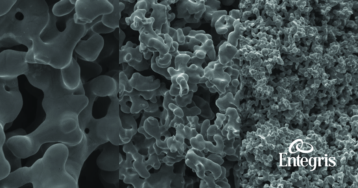
If you asked a semiconductor process engineer to name their biggest challenge when tackling the next technology node, they would likely tell you it is figuring out how to achieve high device yields. This is mainly due to an increase in possible points of contamination as the number of potential contaminants grows and their sizes shrink. It is becoming particularly difficult to detect metal contaminants and pinpoint their root cause so they can be eliminated. That’s because they can form anywhere in the process flow.
In the early days of semiconductor manufacturing, fabs would remove contaminants from their process fluids in a sequence that could be analogized to making a cup of coffee. By using a filter with tiny pores, large contaminants (coffee grounds) are separated from water. Because the coffee grounds are too large to pass through the filter, they can’t pass into the coffee we drink.
Biopharma manufacturing is an essential part of the healthcare industry, producing lifesaving treatments for patients around the world. Traditional manufacturing methods can have a significant environmental impact driven by stainless steel equipment requiring extensive cleaning and sterilization processes that consume substantial amounts of water and energy in addition to cleaning agents.
For decades, the semiconductor device manufacturing mantra was “How do we make them smaller, cheaper, and faster?” The pursuit of Moore’s Law – the doubling of transistors on a chip every two years – was achieved through planar scaling. But that approach could only go on for so long. The mantra now is “How do we improve power, performance, area, and cost (PPAC)?” At the 14 nm node, it was clear that the best way to push the limits of semiconductor device PPAC was to take it into the third dimension.
Things are not always as they appear. Take semiconductor manufacturing. On the surface, it may seem that the secret to making semiconductor devices more advanced lies in the design. But just as an architect’s design for a building may not be structurally feasible without the right materials, a semiconductor device design may not be functional if the materials and their interactions are not considered and optimized.
By: Mike Lamach, Reach-In Sales Leader, FARRAR™ | Trane Technologies The explosion of needs for -80°C through -60°C assets over the past decade has been nothing short of remarkable. Clinical research investments keep expanding while commercial-scale needs continue to transform the landscape.
Here’s a challenge, say the number 9 out loud, nine times. 9, 9, 9, 9, 9, 9, 9, 9, 9.
As the chief technologist for the Life Sciences Division at Trane Technologies, Scott Farrar knows a thing or two about ultra-low temperature control for the life sciences industry, perhaps drawing inspiration from his days at Penn State University enjoying peach ice cream. Scott’s biggest inspiration, however, was his entrepreneurial dad who started a solar equipment company, teaching Scott from a young age the importance of sciences, technology, engineering, and mathematics (STEM) education and solving problems. Scott carried those tools with him, and upon completing his formal education, went to work for a pharmaceutical manufacturing company in research and development, specializing in low-temp freezers and incubators as well as heat-momentum and mass-transfer-type processes for the pharmaceutical industry. His exposure to dilemmas and investigative approach is what drove him to create better customer experiences.
Silicon carbide (SiC) has become popular with chipmakers. Its wide-bandgap structure offers many des...

Powder can be a mess when not delt with properly. Have you ever dropped a bag of flour on the floor ...

Entegris is delighted to announce our new interactive tool intended to help the life sciences indust...

If you asked a semiconductor process engineer to name their biggest challenge when tackling the next...


In the early days of semiconductor manufacturing, fabs would remove contaminants from their process ...

Biopharma manufacturing is an essential part of the healthcare industry, producing lifesaving treatm...

For decades, the semiconductor device manufacturing mantra was “How do we make them smaller, cheaper...

Things are not always as they appear. Take semiconductor manufacturing. On the surface, it may seem ...

By: Mike Lamach, Reach-In Sales Leader, FARRAR™ | Trane Technologies The explosion of needs for -80°...
Here’s a challenge, say the number 9 out loud, nine times. 9, 9, 9, 9, 9, 9, 9, 9, 9.

As the chief technologist for the Life Sciences Division at Trane Technologies, Scott Farrar knows a...
© 2026 Entegris. All Rights Reserved


