

Science that is transforming lives and enabling the future
Scaling New Heights: How Molybdenum is Revolutionizing 3D NAND Architectures
Understanding potential sources of contamination and developing targeted filtration solutions in 30% H2O2
Exploring Entegris POCO Materials EDM-AF5® Graphite In our previous blog post, we reviewed one of our most economical Ultrafine graphite grades, POCO EDM-1. This five-micron grade provides a combination of speed, low electrode wear, and a good surface finish at a much lower price point. Now we’ll venture into the opposite side of the spectrum and explore our POCO EDM-AF5® graphite grade, the smallest particle size grade Entegris POCO Materials offers.
What does an Entegris employee look like? What do they do all day, and what do they like about their jobs? This is part of a series that will take a deep dive into a variety of careers at Entegris. We’ll highlight several employees and their valuable contribution to the organization. What do they do, how are they succeeding, and why do they think Entegris is a great place to work?
Silicon Carbide’s Next Phase: From Expansion to Optimization
Sustainability Challenges Around SiC Polishing Slurry recycling supports cleaner semiconductor manufacturing
What does an Entegris employee look like? What do they do all day, and what do they like about their jobs? This is part of a series that will take a deep dive into a variety of careers at Entegris. We’ll highlight several employees and their valuable contribution to the organization. What do they do, how are they succeeding, and why do they think Entegris is a great place to work?
The Future of Silicon Carbide Manufacturing: Innovations and Techniques
Exploring Entegris POCO Materials EDM-1® Graphite
What does an Entegris employee look like? What do they do all day, and what do they like about their jobs? This blog is part of a series that will take a deep dive into a variety of careers at Entegris. We’ll highlight several employees and their valuable contributions to the organization. What do they do, how are they succeeding, and why do they think Entegris is a great place to work?
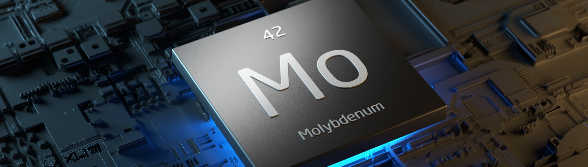
Scaling New Heights: How Molybdenum is Revolutionizing 3D NAND Architectures

Understanding potential sources of contamination and developing targeted filtration solutions in 30%...
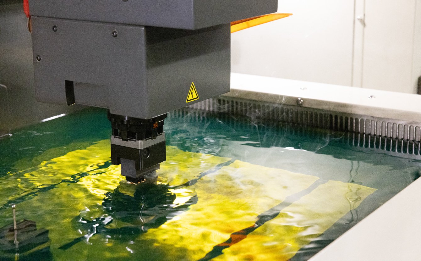
Exploring Entegris POCO Materials EDM-AF5® Graphite In our previous blog post, we reviewed one of ou...

What does an Entegris employee look like? What do they do all day, and what do they like about their...

Silicon Carbide’s Next Phase: From Expansion to Optimization

Sustainability Challenges Around SiC Polishing Slurry recycling supports cleaner semiconductor manuf...

What does an Entegris employee look like? What do they do all day, and what do they like about their...
Looking Back at 60 Years of Moore’s Law
The Future of Silicon Carbide Manufacturing: Innovations and Techniques
Exploring Entegris POCO Materials EDM-1® Graphite
What does an Entegris employee look like? What do they do all day, and what do they like about their...
© 2026 Entegris. All Rights Reserved

