hero-654791312-sized

Ensights

Science that is transforming lives and enabling the future

How to Approach Materials Processing for Scaled Devices

All Posts

How to Approach Materials Processing for Scaled Devices

Setting the stage

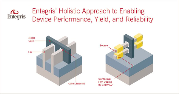
Logic devices are getting smaller, and the introduction of 3D architectures that use vertical fins and nanowires in their gate design introduce more complexity to the fabrication process. As technology nodes shrink beyond 10 nm, new materials are required in both FEOL and BEOL processes to enable performance, yield, reliability and cost.

Approaching implementation

Successful implementation of new device architectures, whether they are nanowire transistor structures or high-layer-count 3D NAND memory, can’t be accomplished merely by substituting one material with a higher-performing option. One change has a cascading effect on the entire process. Changing the interconnect metal, for example, may require new barrier films and thus new clean chemistries. And with each chemistry change, advancements in membrane technology for effective filtration are required.


pictogram-facebook-10639-1200x630

Solution checklist

A complete, holistic solution should address performance, efficiency, reliability, yield, and overall cost of ownership. Whether it is new metallurgy precursors, effective delivery systems, new cleaning formulations, or new filtration membranes, find a holistic solution to your unique integration challenges.


To explore more possibilities for approaching materials processing for scaled devices, check out our recent white paper.


Related Posts

What is the Inkjet Cartridge Effect in Air Filtration Performance?

A “one size fits all” approach for chemical air filtration entails a productivity and safety risk in commercial environments reliant on pure air quality. Trying to use one type of chemical air filter for every scenario may provide protection, but without optimization the protection is both limited and temporary.

Sharing Semiconductor Industry Sustainability Plans at the SEMI Earth Month Lightning Talks

In recognition of Earth Day, SEMI’s Climate Equity & Social Impact Working Group (CESI) organized a series of lighting talks from member organizations to highlight their progress on sustainability. We heard from companies around the semiconductor industry, as well as Entegris engineer Paola Gonzalez. They shared a number of different strategies for mitigating climate impact. Here are some of the key takeaways.

One in a Billion: AMC Filtration Essential to a Safer, Healthy Environment

Airborne molecular contamination (AMC) is common to every environment. These contaminants are not physical particles such as those found in airborne dust or pathogens. AMC is gas molecules that are part of and move with air. These molecules are the result of outgassing or emissions from virtually anything that can be found in a given setting, from humans and animals to equipment, materials and processes, as well as external AMC sources. Sensitivity to these gases varies widely in each environment.