The desire for ever more computing power in a smaller footprint requires transistors that perform faster while consuming less power. However, new materials and architectures developed with these goals in mind are not easy to transfer from research and development to full-scale, high-volume production.
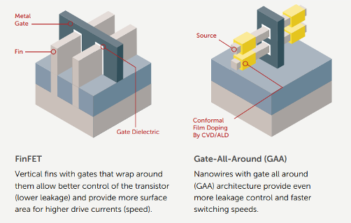
Logic devices are getting smaller, and the introduction of 3D architectures that use vertical fins and nanowires in their gate design introduce more complexity to the fabrication process. As technology nodes shrink beyond 10 nm, new materials are required in both FEOL and BEOL processes to enable performance, yield, reliability and cost.
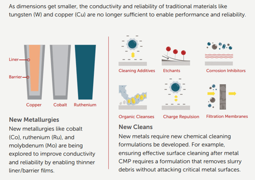
In the Front End of Line, transistors are moving to non-planar 3D structures, like FinFET and Gate-All-Around. In the Back End of Line, metal line widths and pitch are shrinking beyond the limits for traditional metals like copper and tungsten to be effective.
In both cases, new materials must be considered to guarantee performance. However, successful implementation of new device architectures, whether they are nanowire transistor structures or high-layer-count 3D NAND memory, can’t be accomplished merely by substituting one material with a higher-performing option. One change has a cascading effect on the entire process.
New materials that improve one aspect of device performance can negatively affect reliability or throughput unless related downstream changes are implemented. Changing, the interconnect metal, for example, may require new barrier films and this means new etch chemistries and cleans must be developed to ensure yield.
Semiconductor device manufacturers must therefore partner closely with suppliers of everything from metals to etchants to fully understand all the implications of migrating to demanding materials and architectures with challenging geometric constraints.
Contamination must also be kept extremely low throughout the entire process, requiring cutting-edge chemical purity and filtration. This further necessitates close collaboration with materials suppliers to choose appropriate chemical precursors that will optimize the process for a given application.
Ultimately, success will be defined by how fast device manufacturers can innovate to simultaneously achieve high performance, high yield, and low cost.
For more details visit www.entegris.com/holistic.


