hero-654791312-sized

Ensights

Science that is transforming lives and enabling the future

Cars and Chips: The Acceleration of Electronic Systems

All Posts

Cars and Chips: The Acceleration of Electronic Systems

The rapid increase of semiconductors in cars enables significant safety, connectivity, mobility, and sustainability improvements. The standards to measure reliability under the tough conditions a car presents are based on how vehicles operate today. Conventional vehicles are generally idle 95% of the time. As a result, the expected lifetime of the electronics systems is well beyond the lifetime of the vehicle itself. 

If the future of transportation will rely on autonomous vehicles that will rarely be idle, the definition of electronics’ reliability and operating lifetime will significantly change. To better prepare for the change, automakers should look at optimizing reliability in IC (integrated circuit) manufacturing. Our full paper examines the role contamination in the chemicals, process gases, and air in a semiconductor fab has, and its impact on electronic vehicle reliability.

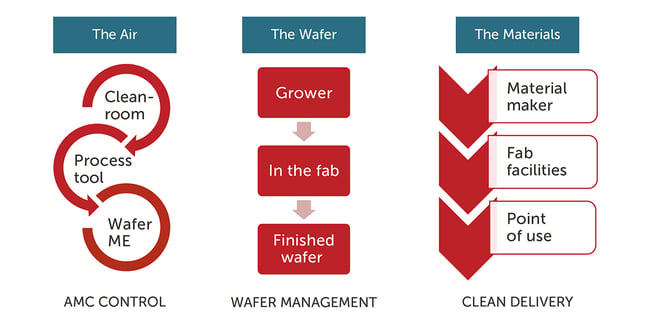
Three areas of impact that should be considered when optimizing contamination management: the ambient air in the fab, the environment that surrounds the wafer during its lifetime, and the integrity of the materials across the clean chemical delivery pathway.

  • Air – In the broad fab environment and the tool mini environments, air is both an ally and an enemy.
  • Wafer – Each transport and storage operation presents an opportunity to safeguard the wafer surface from abrasion and the addition of contaminants.
  • Materials – Contaminants may originate in the chemical manufacturer’s raw materials, may be added along the clean chemical delivery pathway, or may be the result of unexpected reactions.

Contamination management in each of these three areas presents opportunities to limit process variability. The first step in limiting variation is detecting it, which can be difficult when the contaminants causing the variation are hard to identify or are caused by an unexpected event. When a contaminant signature can be detected, it leaves clues to its root cause. Careful examination of these signatures can lead to the optimization of a contamination control strategy to eliminate the root cause, reducing overall defectivity.
blog-feature-11188-1200x600-mc

The automotive manufacturing paradigm shift leads the supply chain to develop electronic systems that meet parts per billion (ppb) failure rates. This requires changing from an electronic component mindset to a system engineering mindset, focused on the validation and verification of these complex electronic systems in the harsh environments they are required to operate. To increase the velocity of change toward this new model, collaboration between semiconductor customers, semiconductor manufacturers, materials suppliers, and equipment suppliers will be the preferred approach to ensure device reliability. Achieving these new manufacturing standards will drive the shift in our transportation habits, increasing safety, mobility, and sustainability.

Read the full paper, Cars and Chips: The Acceleration of Electronic Systems

Related Posts

Exploring the Superiority of Silicon Carbide in Optical Components

Exploring the Superiority of Silicon Carbide in Optical Components Silicon carbide (SiC) is a leading material for high-performance optical components, offering numerous advantages over traditional materials such as glass and metal. Its exceptional specific stiffness, high thermal conductivity, and outstanding dimensional stability position SiC as a superior choice compared to beryllium and low-expansion glass ceramics. Historically, the high costs associated with the preliminary shaping and final finishing of SiC have hindered its widespread adoption in optical systems. The material is both hard and strong, requiring precision machining with expensive diamond tooling on high-quality, rigid machine tools. However, advances in manufacturing techniques, such as near-net-shape slip casting, have demonstrated success in reducing costs despite necessitating significant diamond grinding. Building on this success, Entegris offers an entirely new way of creating SiC. Using our chemical vapor conversion process, we can create net- or near net-shaped SiC components in complex forms while spending much less time on fabrication.

Entegris Offers New FOUP Form-Factors for Non-Standard Wafers

Entegris Offers New FOUP Form-Factors for Non-Standard Wafers Over the last few years, 3D stacking has gone from a relatively niche fabrication method to an absolute necessity for cutting-edge applications. As chipmakers delve into smaller and smaller nodes, stacking and die-bonding wafers has become a preferred way of creating more processing power in a smaller space. Stacked and bonded wafers don’t behave the same way as 2D wafers: Wafers are thinned prior to bonding, which results in wafers that can sag when handled Bonded wafers are thicker and heavier than 2D wafers when assembled Bonded wafers can also warp following assembly Many automation tools rely on the predictable geometry and characteristics of 2D silicon wafers for safe handling and transport. While stacked and bonded wafers are a game-changer for miniaturization, they can also force manufacturing compromises unless chipmakers adopt specialized tools for the back end of the line (BEOL).

Mastering the SiC Wafer Transition

The use of silicon carbide (SiC) semiconductors offers a huge advantage for electric vehicles (EVs) due to lower switching losses and higher efficiencies, but cost has always been a drawback. SiC wafer manufacturing can suffer from high costs and lower yields, causing SiC semiconductors to cost up to eight times more than their silicon equivalents. This cost often gets passed on to the end customer, making EVs more expensive.