
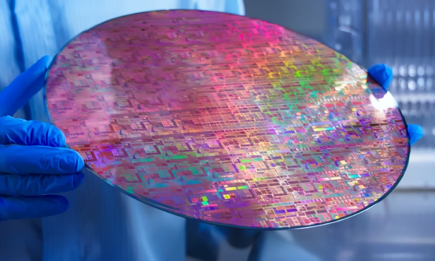
Effect of POU Filter Pore Size on EUV Bridge Defect Density

Science that is transforming lives and enabling the future
Effect of POU Filter Pore Size on EUV Bridge Defect Density
Hydrogen Halides in Semiconductor Manufacturing: Three Gases, Three Distinct Challenges and Solutions
End-to-End Manufacturing Excellence: Seven Questions Every New (or Growing) Fab Team Should Be Asking
Under Pressure: Solving High Viscosity Material Challenges in Advanced Packaging
Cleaner Chemistry and Faster Startup with Next Generation Ancillary Photochemical Filters
Solving Bridge Defects in EUV CAR Resists with Advanced UPE Filtration
Building Resilient Infrastructure to Better Serve Our Customers: A Vision from Abhijeet Bhandare “Our digital transformation is about one thing: being the most reliable, innovative partner for our customers.” – Abhijeet Bhandare
Collaborating to Solve Advanced Packaging Substrate Warpage, Thickness, and Heavy Payload Transport and Shipping Defect Challenges
Airborne molecular contamination (AMC) threatens semiconductor yield and reliability. Learn how Entegris helps fabs detect and control AMC with advanced filtration and data-driven strategies.
Optimizing Wafer Polishing: Innovations in CMP Slurry Characterization and Filtration
Understanding potential sources of contamination and developing targeted filtration solutions in 30% H2O2
Effect of POU Filter Pore Size on EUV Bridge Defect Density

Hydrogen Halides in Semiconductor Manufacturing: Three Gases, Three Distinct Challenges and Solution...
End-to-End Manufacturing Excellence: Seven Questions Every New (or Growing) Fab Team Should Be Askin...

Under Pressure: Solving High Viscosity Material Challenges in Advanced Packaging

Cleaner Chemistry and Faster Startup with Next Generation Ancillary Photochemical Filters

Solving Bridge Defects in EUV CAR Resists with Advanced UPE Filtration

Building Resilient Infrastructure to Better Serve Our Customers: A Vision from Abhijeet Bhandare “Ou...

Collaborating to Solve Advanced Packaging Substrate Warpage, Thickness, and Heavy Payload Transport ...

Airborne molecular contamination (AMC) threatens semiconductor yield and reliability. Learn how Ente...

Optimizing Wafer Polishing: Innovations in CMP Slurry Characterization and Filtration


Understanding potential sources of contamination and developing targeted filtration solutions in 30%...
© 2026 Entegris. All Rights Reserved

