hero-654791312-sized

Ensights

Science that is transforming lives and enabling the future

A Look Back at 2018

All Posts

A Look Back at 2018

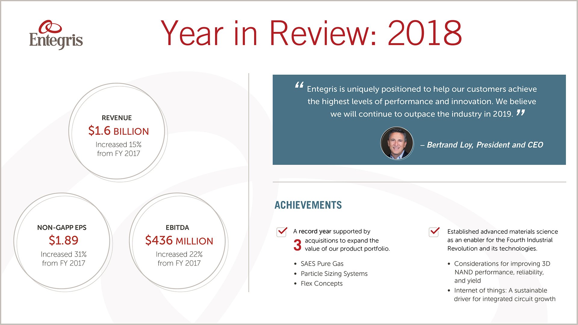
We are proud of our accomplishments in 2018 and we are looking ahead to what we can achieve in 2019.

We brought on board three companies that helped expand our portfolio and impact on the technologies of the Fourth Industrial Revolution. Our great teams of scientists and engineers created solutions alongside our customers to help fuel innovation. And, most importantly, we helped the industry recognize the importance of advanced materials science in enabling the technologies of the future.

We are looking forward to 2019; a year we believe technology will take a back seat to science. New, advanced materials and the science behind the innovations that people depend on will be center stage.

We have a lot of work ahead of us but our team is ready for the challenges ahead and ready to push the industry to achieve standards never thought possible.
 
10348-facebook-1920x1080

Visit our news page to learn more about our 2018 achievements and announcements. 


Related Posts

Exploring the Superiority of Silicon Carbide in Optical Components

Exploring the Superiority of Silicon Carbide in Optical Components Silicon carbide (SiC) is a leading material for high-performance optical components, offering numerous advantages over traditional materials such as glass and metal. Its exceptional specific stiffness, high thermal conductivity, and outstanding dimensional stability position SiC as a superior choice compared to beryllium and low-expansion glass ceramics. Historically, the high costs associated with the preliminary shaping and final finishing of SiC have hindered its widespread adoption in optical systems. The material is both hard and strong, requiring precision machining with expensive diamond tooling on high-quality, rigid machine tools. However, advances in manufacturing techniques, such as near-net-shape slip casting, have demonstrated success in reducing costs despite necessitating significant diamond grinding. Building on this success, Entegris offers an entirely new way of creating SiC. Using our chemical vapor conversion process, we can create net- or near net-shaped SiC components in complex forms while spending much less time on fabrication.

Entegris Offers New FOUP Form-Factors for Non-Standard Wafers

Entegris Offers New FOUP Form-Factors for Non-Standard Wafers Over the last few years, 3D stacking has gone from a relatively niche fabrication method to an absolute necessity for cutting-edge applications. As chipmakers delve into smaller and smaller nodes, stacking and die-bonding wafers has become a preferred way of creating more processing power in a smaller space. Stacked and bonded wafers don’t behave the same way as 2D wafers: Wafers are thinned prior to bonding, which results in wafers that can sag when handled Bonded wafers are thicker and heavier than 2D wafers when assembled Bonded wafers can also warp following assembly Many automation tools rely on the predictable geometry and characteristics of 2D silicon wafers for safe handling and transport. While stacked and bonded wafers are a game-changer for miniaturization, they can also force manufacturing compromises unless chipmakers adopt specialized tools for the back end of the line (BEOL).

Mastering the SiC Wafer Transition

The use of silicon carbide (SiC) semiconductors offers a huge advantage for electric vehicles (EVs) due to lower switching losses and higher efficiencies, but cost has always been a drawback. SiC wafer manufacturing can suffer from high costs and lower yields, causing SiC semiconductors to cost up to eight times more than their silicon equivalents. This cost often gets passed on to the end customer, making EVs more expensive.