hero-654791312-sized

Ensights

Science that is transforming lives and enabling the future

How Predictable is Your Lithography Process?

All Posts

How Predictable is Your Lithography Process?

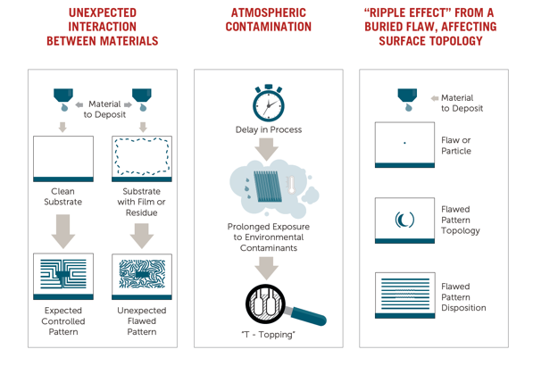
Lithographer’s face the challenge to translate designs into reproducible patterns that meet their yield, parametric performance, and reliability goals. Success or failure relies heavily on the controls in place that limit process variation. Recognizing and addressing all the sources of lithography pattern variations can preoccupy lithographers.


Hence the question, where can pattern flaws originate?


Lithography

 Click the image to see this process in motion


You’re not alone in mitigating these challenges.  Collaboration between fabs, equipment makers, materials suppliers, and designers can lead to a more holistic approach to finding the root cause.


Join the conversation at www.entegris.com/pattern to identify the sources of your pattern integrity challenges.


Related Posts

Entegris Offers New FOUP Form-Factors for Non-Standard Wafers

Entegris Offers New FOUP Form-Factors for Non-Standard Wafers Over the last few years, 3D stacking has gone from a relatively niche fabrication method to an absolute necessity for cutting-edge applications. As chipmakers delve into smaller and smaller nodes, stacking and die-bonding wafers has become a preferred way of creating more processing power in a smaller space. Stacked and bonded wafers don’t behave the same way as 2D wafers: Wafers are thinned prior to bonding, which results in wafers that can sag when handled Bonded wafers are thicker and heavier than 2D wafers when assembled Bonded wafers can also warp following assembly Many automation tools rely on the predictable geometry and characteristics of 2D silicon wafers for safe handling and transport. While stacked and bonded wafers are a game-changer for miniaturization, they can also force manufacturing compromises unless chipmakers adopt specialized tools for the back end of the line (BEOL).

Mastering the SiC Wafer Transition

The use of silicon carbide (SiC) semiconductors offers a huge advantage for electric vehicles (EVs) due to lower switching losses and higher efficiencies, but cost has always been a drawback. SiC wafer manufacturing can suffer from high costs and lower yields, causing SiC semiconductors to cost up to eight times more than their silicon equivalents. This cost often gets passed on to the end customer, making EVs more expensive.

What is the Inkjet Cartridge Effect in Air Filtration Performance?

A “one size fits all” approach for chemical air filtration entails a productivity and safety risk in commercial environments reliant on pure air quality. Trying to use one type of chemical air filter for every scenario may provide protection, but without optimization the protection is both limited and temporary.