hero-654791312-sized

Ensights

Science that is transforming lives and enabling the future

Global Internet of Things Day

All Posts

Global Internet of Things Day


IoT

Today, Entegris recognizes a milestone event in the semiconductor industry.

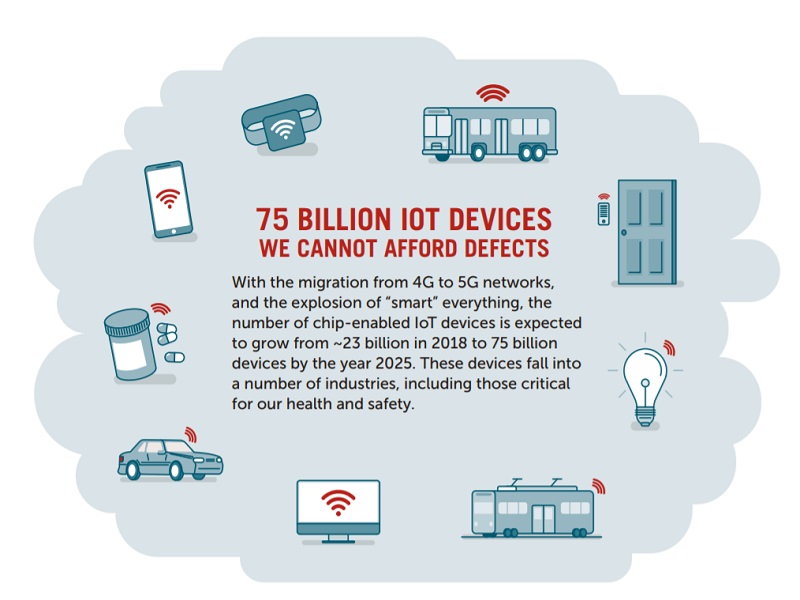
Global Internet of Things Day was first initiated by the IoT Council in 2010. It serves as an invitation to communities around the world to discuss the implications and visions for the future of IoT. The event has grown in scale and scope as advancements in smart devices connected to wireless networks (4G/5G), WiFi networks, and near field communications (NFC, RFID, Bluetooth) continue to be integrated into our everyday lives.


According to our Chief Technology Officer, Jim O'Neill, it's not enough to simply build out capacity to satisfy this demand; superior reliability and performance and IC components specific to each application also need to be considered.


The time has come for our industry to adjust its mindset and proactively address the key challenges brought on by these new technologies. It will take collaboration from across the supply chain to meet capacity, cost, performance, yield and reliability demands. By working together, higher standards will be set and the industry will be better positioned to achieve things only previously imagined.


To learn more about IoT and the challenges the industry must overcome to drive innovation, visit www.entegris.com/IoT.


Related Posts

Entegris Offers New FOUP Form-Factors for Non-Standard Wafers

Entegris Offers New FOUP Form-Factors for Non-Standard Wafers Over the last few years, 3D stacking has gone from a relatively niche fabrication method to an absolute necessity for cutting-edge applications. As chipmakers delve into smaller and smaller nodes, stacking and die-bonding wafers has become a preferred way of creating more processing power in a smaller space. Stacked and bonded wafers don’t behave the same way as 2D wafers: Wafers are thinned prior to bonding, which results in wafers that can sag when handled Bonded wafers are thicker and heavier than 2D wafers when assembled Bonded wafers can also warp following assembly Many automation tools rely on the predictable geometry and characteristics of 2D silicon wafers for safe handling and transport. While stacked and bonded wafers are a game-changer for miniaturization, they can also force manufacturing compromises unless chipmakers adopt specialized tools for the back end of the line (BEOL).

Mastering the SiC Wafer Transition

The use of silicon carbide (SiC) semiconductors offers a huge advantage for electric vehicles (EVs) due to lower switching losses and higher efficiencies, but cost has always been a drawback. SiC wafer manufacturing can suffer from high costs and lower yields, causing SiC semiconductors to cost up to eight times more than their silicon equivalents. This cost often gets passed on to the end customer, making EVs more expensive.

What is the Inkjet Cartridge Effect in Air Filtration Performance?

A “one size fits all” approach for chemical air filtration entails a productivity and safety risk in commercial environments reliant on pure air quality. Trying to use one type of chemical air filter for every scenario may provide protection, but without optimization the protection is both limited and temporary.